Semiconductor lithography process

a semiconductor and lithography technology, applied in the field of lithography process, can solve the problems of difficult to achieve enough resolution, reduce the efficiency of lithography, so as to achieve the effect of higher dosage and higher dosag

Active Publication Date: 2011-10-13
NAN YA TECH
View PDF1 Cites 21 Cited by
  • Summary
  • Abstract
  • Description
  • Claims
  • Application Information

AI Technical Summary

Benefits of technology

[0008]It is one object of the invention to provide an improved exposure method in order to solve the above-mentioned shortcomings of the prior art.
[0009]According to the claimed invention, a semiconductor lithography process includes providing a substrate; coating the substrate with a photoresist film; subjecting the photoresist film to a flood exposure to blanket expose the photoresist film across the substrate to a first radiation with a relatively lower dosage; subjecting the photoresist film to a main exposure using a photomask to expose the photoresist film in a step and scan manner to a second radiation with a relatively higher dosage; and developing the photoresist film.
[0010]According to another embodiment of this invention, a semiconductor lithography process includes providing a substrate; coating the substrate with a photoresist film; subjecting the photoresist film to a petit exposure to expose the photoresist film in a step and scan manner to a first radiation with a relatively lower dosage; subjecting the photoresist film to a main exposure using a photomask to expose the photoresist film in the step and scan manner to a second radiation with a relatively higher dosage; and developing the photoresist film.

Problems solved by technology

However, the rate of shrinkage in device pattern is so fast that it has become difficult to achieve enough resolution only by reduction of exposure wavelength.
Given that EUV is a technology requiring high source power, the throughput is limited.

Method used


Image

  • Semiconductor lithography process
  • Semiconductor lithography process
  • Semiconductor lithography process

Examples


Embodiment Construction

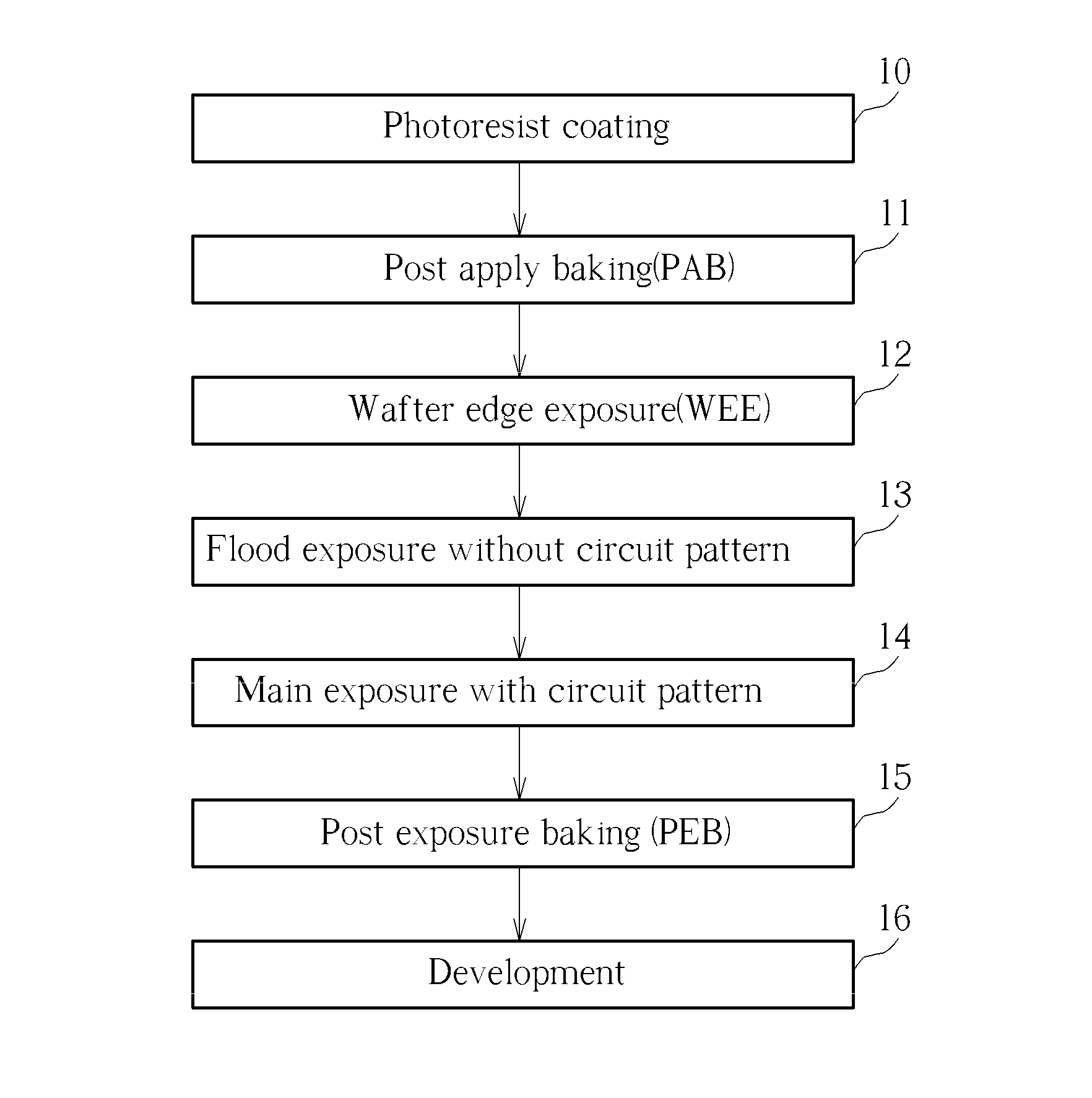
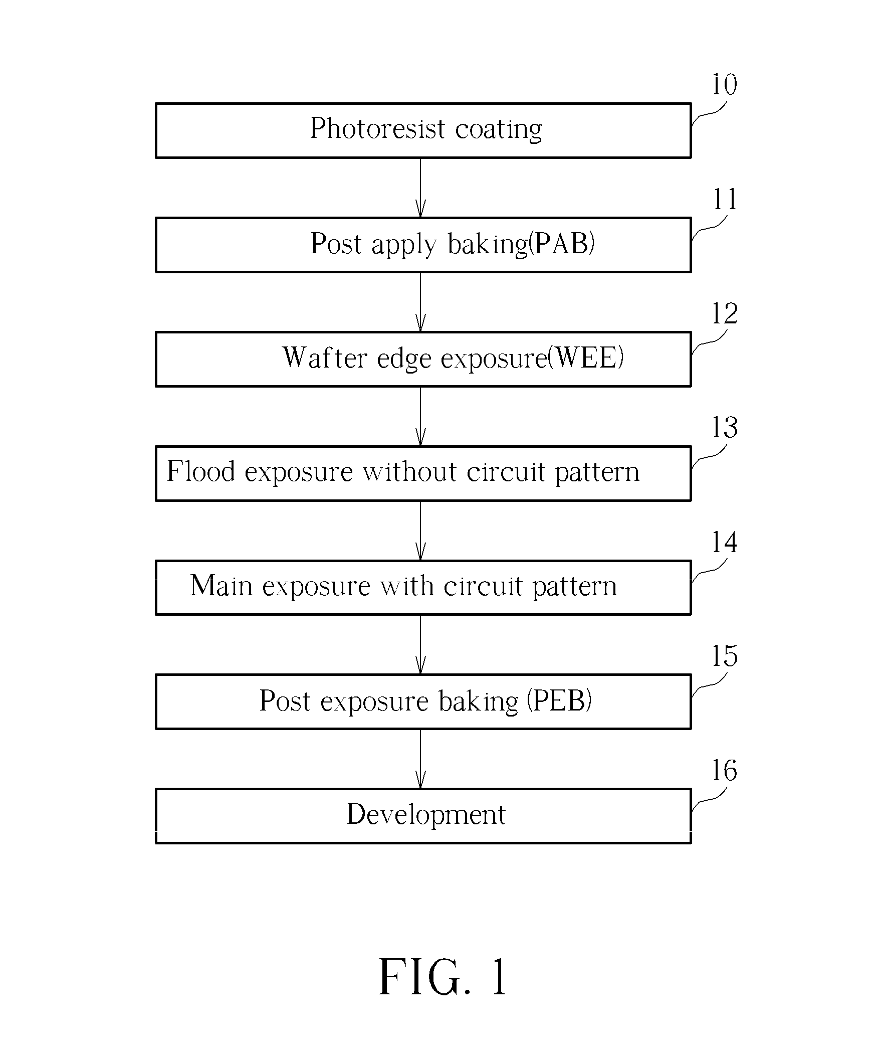
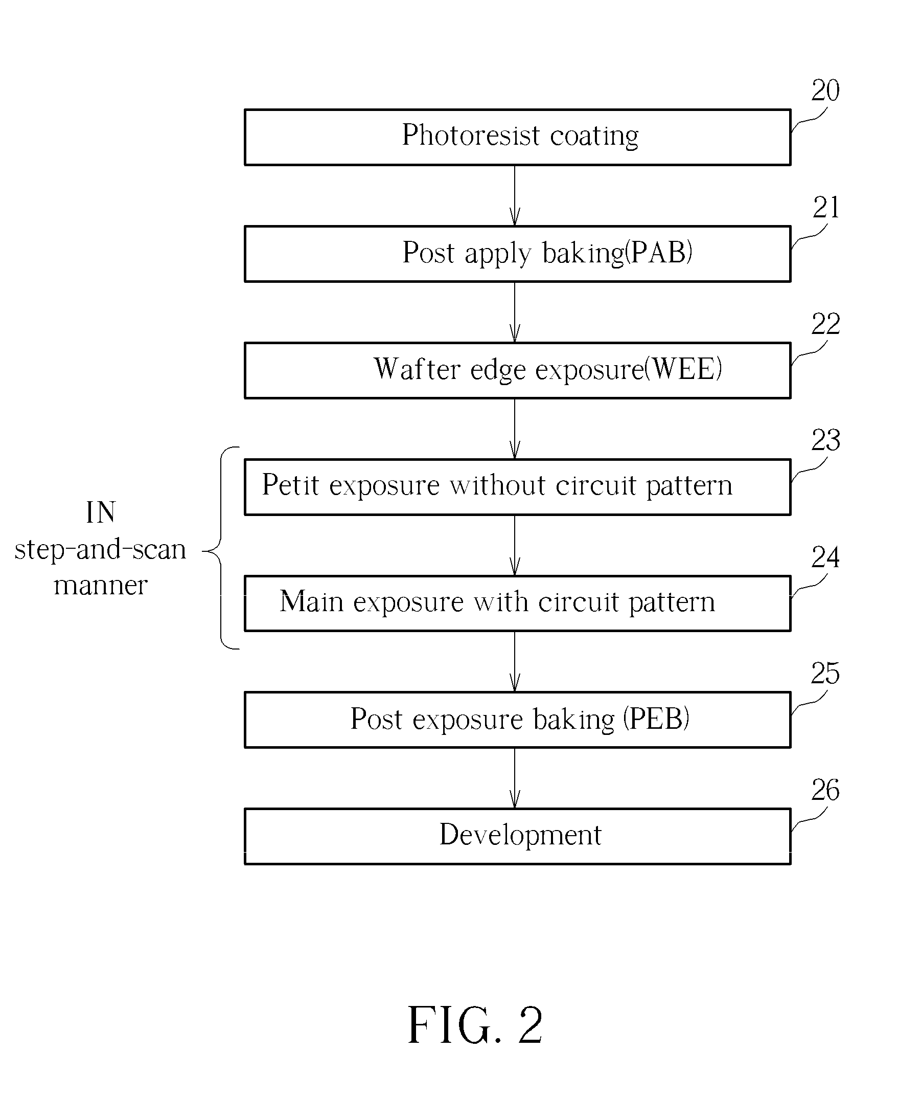
[0015]In the following detailed description of the invention, reference is made to the accompanying drawings which form a part hereof, and in which is shown, by way of illustration, specific embodiments in which the invention may be practiced. These embodiments are described in sufficient detail to enable those skilled in the art to practice the invention. Other embodiments may be utilized without departing from the scope and spirit of the present invention. The terms wafer and substrate used herein include any structure having an exposed surface onto which a layer is deposited according to the present invention, for example, to form the integrated circuit (IC) structure. The term substrate is understood to include semiconductor wafers. The term substrate is also used to refer to semiconductor structures during processing, and may include other layers that have been fabricated thereupon. Both wafer and substrate include doped and undoped semiconductors, epitaxial semiconductor layer...


PUM

PropertyMeasurementUnit
temperatureaaaaaaaaaa
wavelengthaaaaaaaaaa

Abstract

A semiconductor lithography process. A photoresist film is coated on a substrate. The photoresist film is subjected to a flood exposure to blanket expose the photoresist film across the substrate to a first radiation with a relatively lower dosage. The photoresist film is then subjected to a main exposure using a photomask to expose the photoresist film in a step and scan manner to a second radiation with a relatively higher dosage. After baking, the photoresist film is developed.

Description

BACKGROUND OF THE INVENTION[0001]1. Field of the Invention[0002]The present invention relates generally to a lithographic process used in the semiconductor manufacturing process. More particularly, the present invention relates to a double-exposure method that is capable of elongating the lifetime of the radiation source in a lithographic system without affecting the critical dimension (CD) of the circuit features.[0003]2. Description of the Prior Art[0004]Photolithographic technology plays an important role in the manufacture of integrated circuit (IC) chips. Continued improvements in optical projection lithography have enabled the printing of ever-finer features of integrated circuits. This, in turn, has allowed the integrated circuit industry to produce ever more powerful and cost-effective semiconductor devices.[0005]In the field of optical lithographic processing, a photosensitive material is applied to a silicon substrate wafer and then allowed to dry. An exposure tool is util...

Claims


Application Information

Patent Timeline
Patent Type & Authority Applications(United States)
IPC IPC(8): G03F7/20
CPCG03F7/2022G03F7/2028Y10S430/143G03F7/70466G03F7/70425
Inventor HUANG, PEI-LINHUANG, CHUN-YENWANG, YI-MING
Owner NAN YA TECH
Why Eureka
Try Eureka