Method of fabricating mems, nems, photonic, micro- and nano-fabricated devices and systems

a technology of applied in the field of manufacturing mems, nems, photonic, micro- and nano-fabricated devices and systems, can solve the problems of unfulfilled true potential of these technologies, unattractive and risky commercialization of technologies relying on customer micro- and nano-fabrication, and limited products, etc., to achieve faster rate, improve implementation, and reduce costs

Active Publication Date: 2011-10-13
FOR NAT RES INITIATIVES
View PDF0 Cites 14 Cited by
  • Summary
  • Abstract
  • Description
  • Claims
  • Application Information

AI Technical Summary

Benefits of technology

[0012]Through the employment of standardized process modules or building blocks, the implementation of a wide variety of different device types can be performed at lower cost and at a faster rate than is currently possible in the present state of the art.
[0013]The present invention allows design and process rules to be created wherein the design of devices can be automated and thereby greatly improving implementation over the current state of the art.
[0014]Even in situations wherein the process sequence for a device implementation cannot be completely performed using process modules of the present invention, the present invention allows the process sequence to employ process modules for a portion of the process sequence, thereby greatly improving implementation over the current state of the art.

Problems solved by technology

Nevertheless, these products are mostly limited to a few high volume markets in a few selected application domains, due to the enormous cost and time it takes to develop a manufacturing process using these technologies.
Consequently, the true potential of these technologies is still unfulfilled for various low volume applications.
Additionally, even for high-volume markets, the time and cost it takes to develop and take a device into production, as well as the unpredictability of such time and cost, makes commercialization of technologies that rely on customer micro- and nano-fabrication unattractive and risky.
As a result of the enormous cost (e.g., tens to hundreds of millions of dollars) and time (e.g., 3 years or more) it has traditionally taken for products based on these technologies to be designed, developed and reach the marketplace, even the very large volume markets have shown an unattractive return on investment.
For small volume markets, access to these important technologies is thus limited.
A major obstacle in the implementation of devices and systems employing these technologies is the lack of properly defined and standardized fabrication toolsets for the implementation of development prototypes as well as in production.
Additionally, it also may be necessary to develop individual processing steps in the process sequence, thereby increasing cost even more.
Indeed, the inevitable and undesirable outcome of this approach is that these endeavors are prohibitively costly, time consuming, and much more risky than desirable.

Method used


Image

  • Method of fabricating mems, nems, photonic, micro- and nano-fabricated devices and systems
  • Method of fabricating mems, nems, photonic, micro- and nano-fabricated devices and systems
  • Method of fabricating mems, nems, photonic, micro- and nano-fabricated devices and systems

Examples


Embodiment Construction

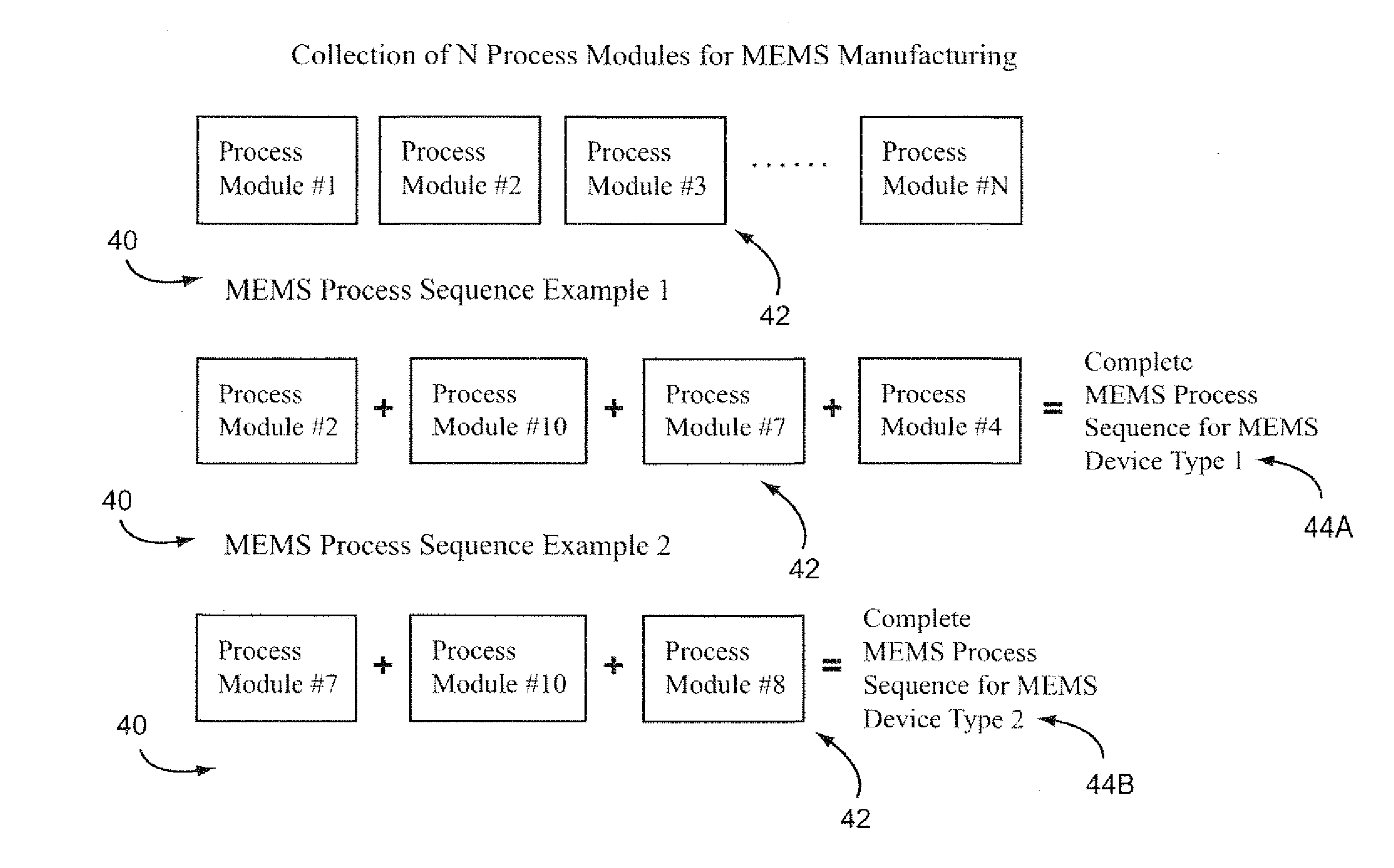
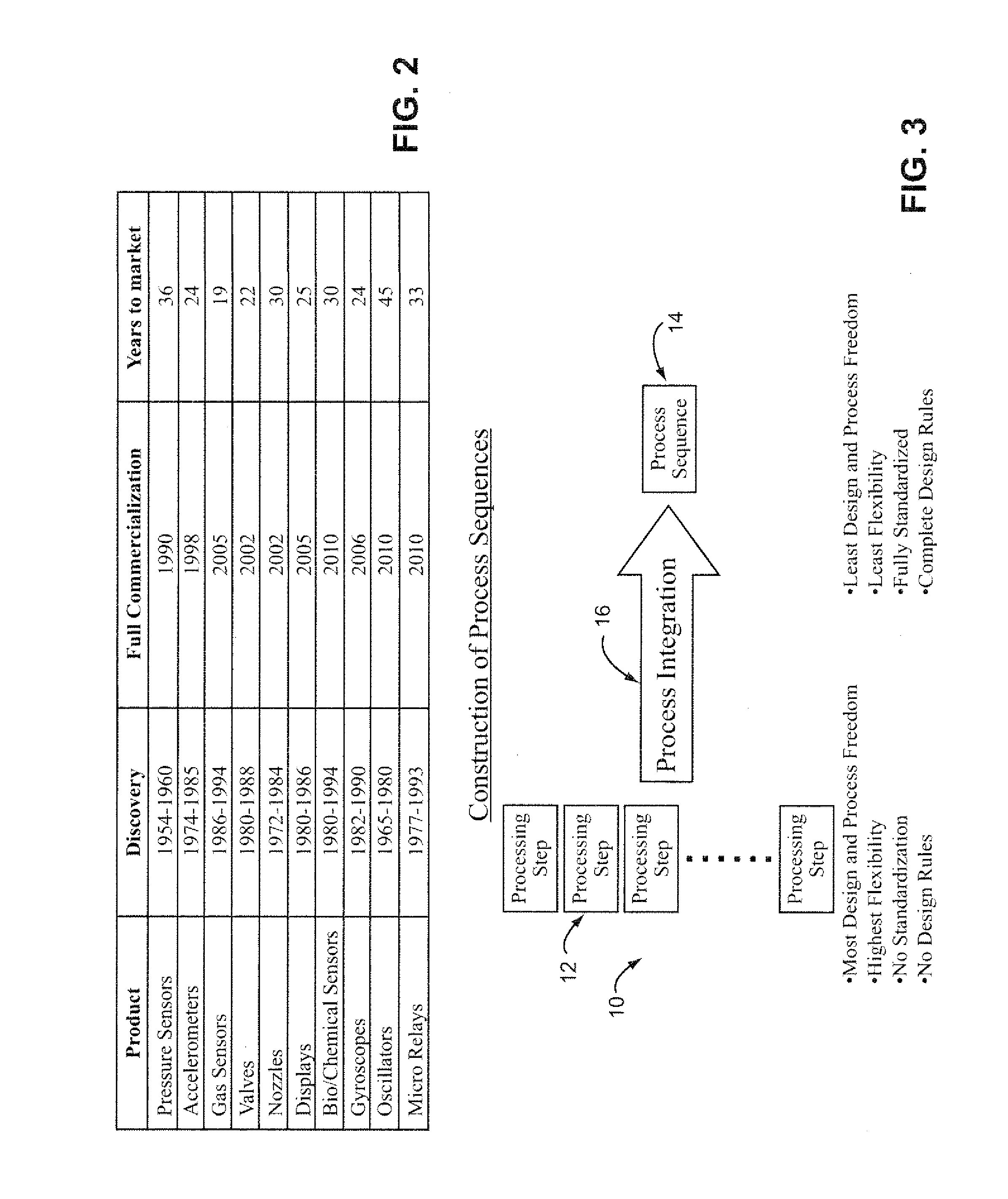
[0029]The present invention is directed to an improved method for the fabrication of Micro-Electro-Mechanical Systems (MEMS), Nano-Electro-Mechanical Systems (NEMS), Photonic, Micro- and Nano-Fabricated Devices and Systems for both rapid prototyping development and manufacturing. In addition, the present invention is applicable to any field of endeavor in which fabrication processes use semiconductor or semiconductor-like processing techniques and use-customized process sequences.

[0030]Despite the enormous economic and strategic merits of technologies that use micro- and nano-fabrication techniques for implementation, the industries based on these technologies have grown at a much slower rate than predicted by experts. This is primarily a result of the cost and time it takes to develop for market, devices and products using these technologies, which is a direct consequence of the lack of well-established, well-defined and standardized process technologies. In current practice, a des...


PUM


Abstract

An improved method for the fabrication of Micro-Electro-Mechanical Systems (MEMS), Nano-Electro-Mechanical Systems (NEMS), Photonics, Nanotechnology, 3-Dimensional Integration, Micro- and Nano-Fabricated Devices and Systems for both rapid prototyping development and manufacturing is disclosed. The method includes providing a plurality of different standardized and repeatable process modules usable in fabricating the devices and systems, defining a process sequence for fabricating a predefined one of the devices or systems, and identifying a series of the process modules that are usable in performing the defined process sequence and thus in fabricating the predefined device or system.

Description

CROSS-REFERENCE TO RELATED APPLICATIONS[0001]This application claims the benefit of U.S. Provisional Application No. 61 / 318,516, filed Mar. 29, 2010, the entire contents of which are incorporated herein by reference.FIELD OF INVENTION[0002]The present invention is directed to an improved method for the fabrication of Micro-Electro-Mechanical Systems (MEMS), Nano-Electro-Mechanical Systems (NEMS), Photonics, Nanotechnology, 3-Dimensional Integration, and Micro- and Nano-Fabricated Devices and Systems for both rapid prototyping development and manufacturing. In addition, the present invention is applicable to any field of endeavor whereby the fabrication processes use semiconductor or semiconductor-like processing techniques and use-customized process sequences.BACKGROUND OF THE INVENTION[0003]Advances in Micro-Electro-Mechanical Systems (MEMS), Nano-Electro-Mechanical Systems (NEMS), Photonic, as well as any devices or systems employing Micro- and Nano-Fabricated technology in their ...

Claims


Application Information

Patent Timeline
Patent Type & Authority Applications(United States)
IPC IPC(8): H01L21/66G06F17/50
CPCB81C99/006
Inventor HUFF, MICHAEL A.
Owner FOR NAT RES INITIATIVES
Why Eureka
Try Eureka