Light emitting device

a technology of light emitting device and light source, which is applied in the direction of semiconductor devices, basic electric elements, electrical appliances, etc., can solve the problems of affecting the preventing and not sufficiently considering the placement of protection elements, so as to improve the light extraction efficiency of light emitting devices, prevent the destruction of element performance and deterioration of performance of light emitting elements, and reduce the loss of output light

Active Publication Date: 2011-10-20
NICHIA CORP
View PDF4 Cites 62 Cited by
  • Summary
  • Abstract
  • Description
  • Claims
  • Application Information

AI Technical Summary

Benefits of technology

[0027]With this arrangement, by forming the light reflecting resin such as to cover a part of the margin of the mounting area 1a, it is prevented that an area, where the substrate is exposed, is formed between the wiring sections and the metal film on the mounting area. Thus, light that is output from the light emitting elements can be reflected all inside the area where the light reflecting resin is formed, and the loss in the output light can be reduced to the maximum to improve the light extraction efficien

Problems solved by technology

However, in a conventional technology, the position of arranging a protection element has not been sufficiently considered in a case of arranging a plurality of elements on a substrate.
For example, in the Unexamined Japanese Patent Application Publication No. 2006-295085 and the Unexamined Japanes

Method used


Image

  • Light emitting device
  • Light emitting device
  • Light emitting device

Examples


first embodiment

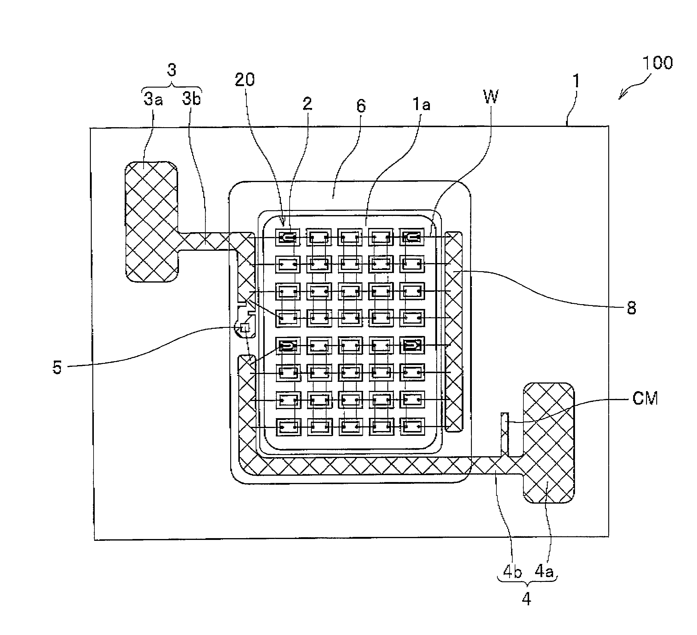
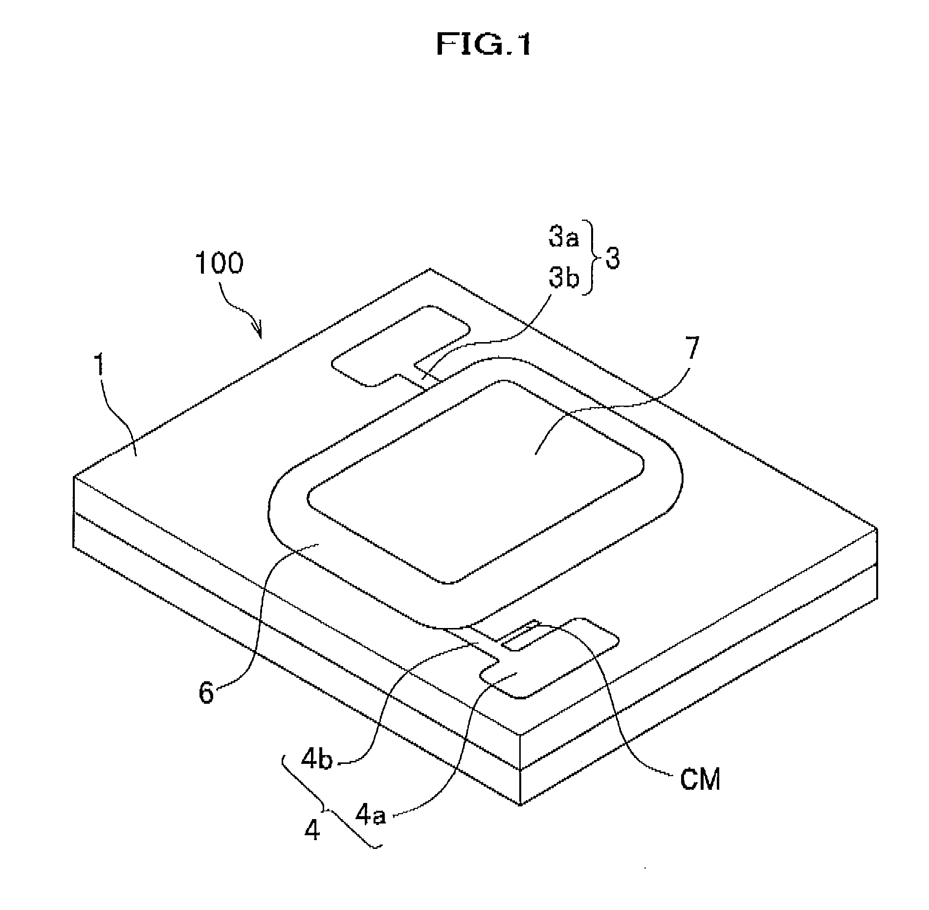
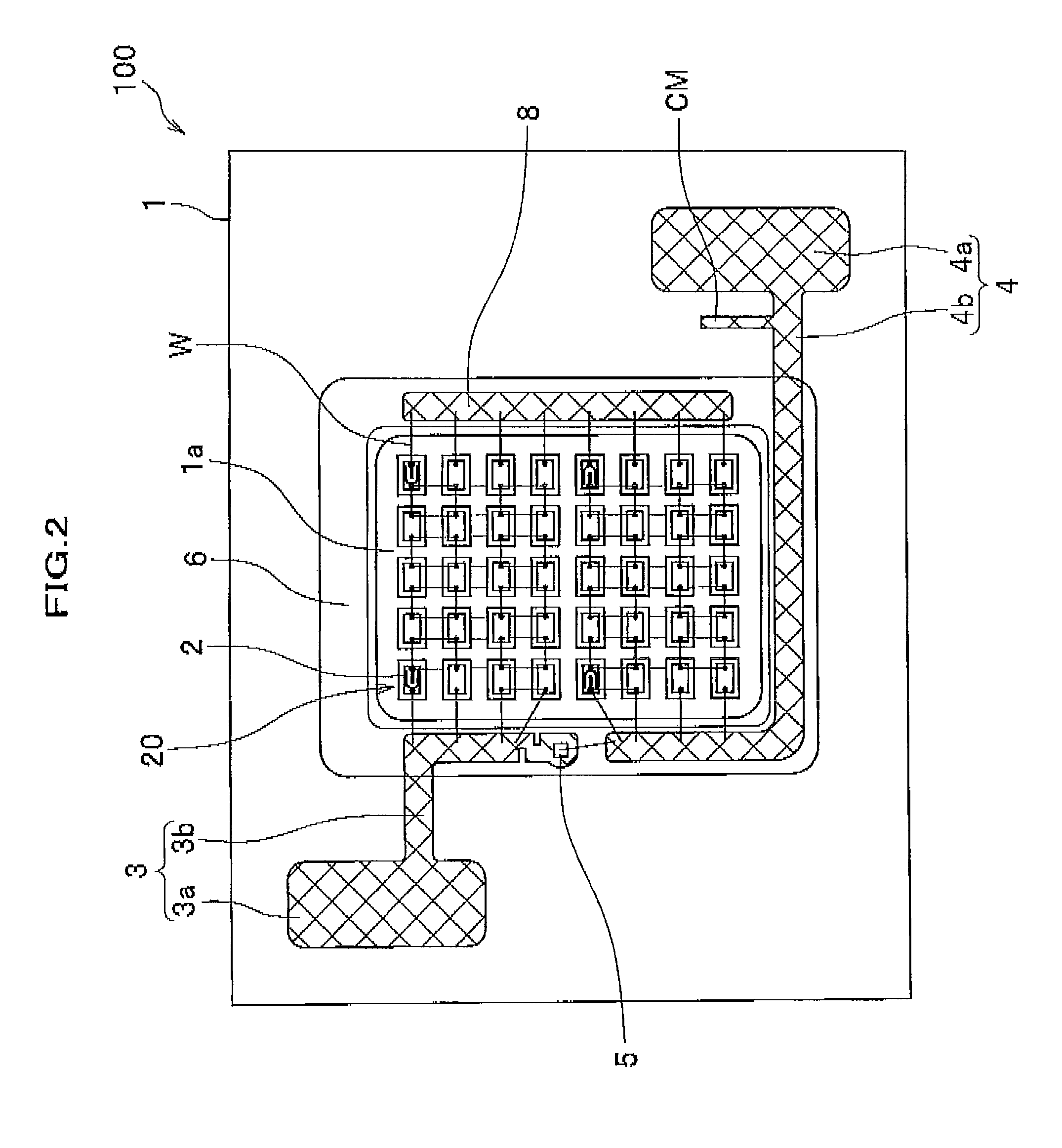
[0039]A light emitting device 100 according to a first embodiment will be described in detail, referring to FIGS. 1 to 4. In the description below, the entire configuration of the light emitting device 100 will be described first, and then respective configurations will be described. For the convenience of description, a light reflecting resin 6 in FIG. 2 is represented by the outline thereof by lines and curves, and shown in a transparent state. In FIGS. 5 to 9 referred to by other embodiments, a light reflecting resin 6 is likewise shown in a transparent state.

Entire Configuration

[0040]The light emitting device 100 is a device used for a lighting device, such as an LED bulb, a display unit, a display, the back light source of a liquid crystal display, and the like. As shown in FIGS. 1, 2, and 4, the light emitting device 100 mainly includes a substrate 1, a plurality of light emitting elements 2 arranged in a mounting area 1a of the substrate 1, a positive electrode 3 and a negati...

second embodiment

[0099]A light emitting device 101 in a second embodiment will be described below, referring to FIG. 5. The light emitting device 101 has, as shown in FIG. 5, a configuration similar to that of the above-described light emitting device 100 in the first embodiment except the state of wiring of wires W. Accordingly, overlapped elements with those of the above-described light emitting device 100 will be given with the same symbols, and description of them will be omitted. Further, the light emitting device 101 has the same entire configuration (FIG. 1) and the same configuration of light emitting elements (FIG. 3) as those of the above-described light emitting device 100, and accordingly description of these will be omitted.

[0100]In the light emitting device 101, as shown in FIG. 5, light emitting elements 2 adjacent to each other in the horizontal and vertical directions with respect to a mounting area 1a are electrically connected by conductive wires W serially and in parallel. As sho...

third embodiment

[0104]A light emitting device 102 in a third embodiment will be described in detail, referring to FIG. 6. The light emitting device 102 has, as shown in FIG. 6, a configuration similar to that of the above-described light emitting device 100 in the first embodiment except the shapes of a wiring section 3b and a wiring section 4b and the state of wiring of wires W. Accordingly, overlapped elements with those of the above-described light emitting device 100 will be given with the same symbols, and description of them will be omitted. Further, the light emitting device 102 has the same entire configuration (FIG. 1) and the same configuration of light emitting elements (FIG. 3) as those of the above-described light emitting device 100, and accordingly description of these will be omitted.

[0105]In the light emitting device 102, as shown in FIG. 6, one end portions of the wiring section 3b and the wiring section 4b are formed adjacent to each other at a corner portion of a substantially r...


PUM


Abstract

There is presented a light emitting device, having plural light emitting elements disposed on a substrate, in which a protection element, such as a zener diode, can be disposed at an appropriate position. The light emitting device includes: a substrate; a light emitting section having plural light emitting elements disposed in a mounting area on the substrate; a positive electrode and negative electrode each having a pad section and wiring section to apply voltage to the light emitting section through the wiring sections; a protection element disposed at one of the positive electrode and negative electrode and electrically connected with the other one electrode; and a light reflecting resin formed on the substrate such as to cover at least the wiring sections and the protection element, wherein the wiring sections are formed along the periphery of the mounting area such that one end portions thereof are adjacent to each other.

Description

CROSS REFERENCE TO RELATED APPLICATION[0001]The application claims the foreign priority benefit under Title 35, United States Code, Section 119(a)-(d) of Japanese Patent Application No. 2010-094718 filed on Apr. 16, 2010 and Japanese Patent Application No. 2011-069193 filed on Mar. 28, 2011 the contents of which are hereby incorporated by reference.BACKGROUND OF THE INVENTION[0002]1. Field of the Invention[0003]The present invention relates to a light emitting device usable for a lighting device such as an LED bulb, a display unit, a display, the back light source of a liquid crystal display, and the like.[0004]2. Description of the Related Art[0005]In recent years, various kinds of light emitting devices using LEDs (light emitting diodes) as light emitting elements have been developed, because the amount of heat generation and the power consumption by LEDs are smaller than those of light sources by a filament bulb or the like, and LEDs have a longer life.[0006]For example, Unexamin...

Claims


Application Information

Patent Timeline
IPC IPC(8): H01L33/08
CPCH01L25/0753H01L2224/48137H01L33/62H01L33/60H01L33/32
Inventor SASANO, HARUAKI
Owner NICHIA CORP
Why Eureka
Try Eureka