Reference voltage generation circuit, drive device, print head, and image forming apparatus
a reference voltage and drive device technology, applied in logic circuit coupling/interface arrangement, pulse technique, instruments, etc., can solve the problems of large variance in power source voltage, variance in print density, printing problem, etc., to reduce the variance in reference voltage, stably drive the driven element, and high quality
- Summary
- Abstract
- Description
- Claims
- Application Information
AI Technical Summary
Benefits of technology
Problems solved by technology
Method used
Image
Examples
first embodiment
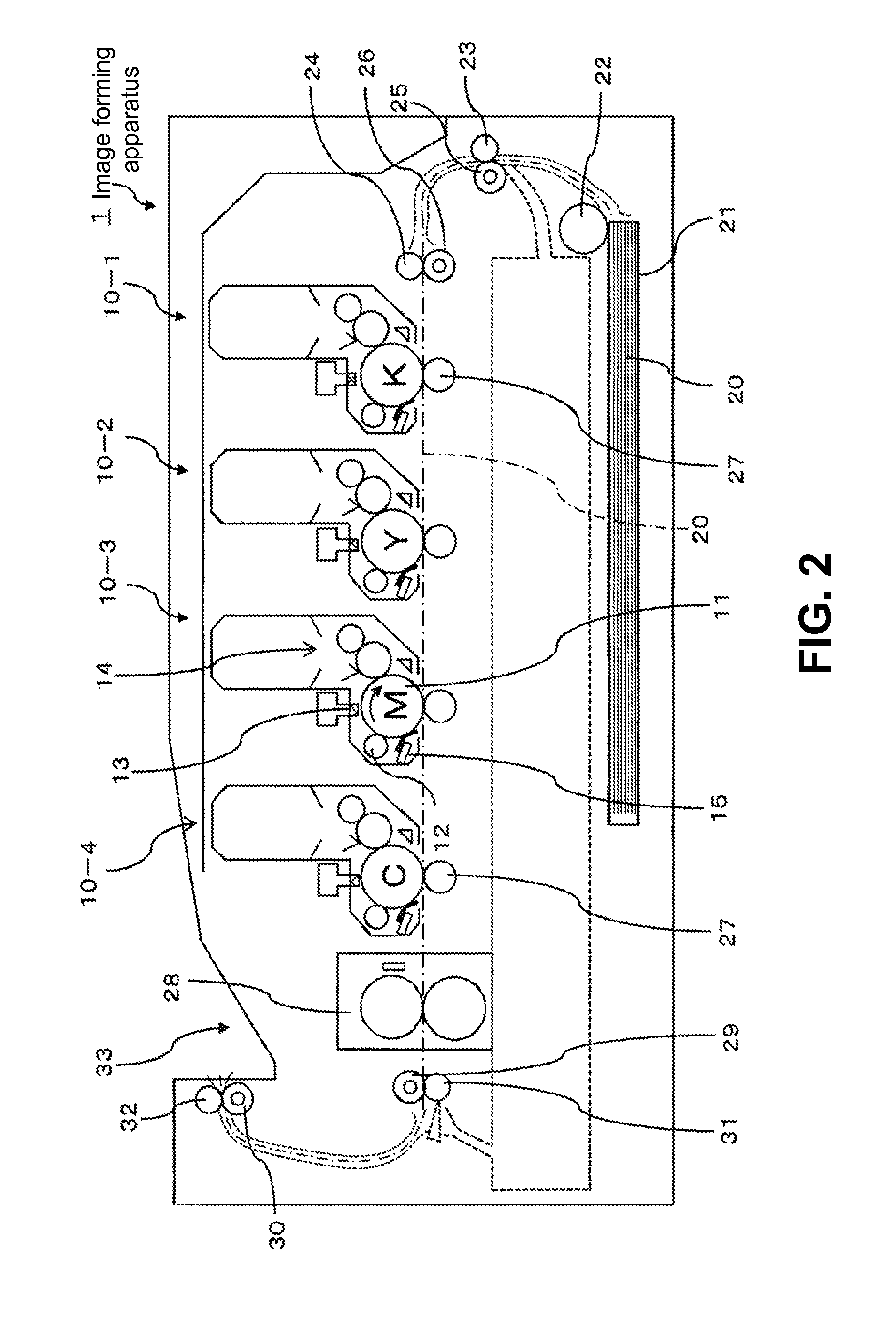
[0041]A first embodiment of the present invention will be explained. FIG. 2 is a schematic sectional view showing a configuration of an image forming apparatus 1 according to the first embodiment of the present invention.
[0042]In the embodiment, the image forming apparatus 1 is an electro-photography type color printer. In the electro-photography type color printer, print heads 13 using a light emitting element (for example, an LED) as a driven element are disposed.
[0043]As shown in FIG. 2, the image forming apparatus 1 includes four process units 10-1 to 10-4 for forming images in colors of black (K), yellow (Y), magenta (M), and cyan (C). The process units 10-1 to 10-4 are arranged from an upstream side in this order along a transportation path of a recording medium 20 (for example, a sheet). The process units 10-1 to 10-4 have an identical internal configuration, and an internal configuration of the process unit 10-3 for magenta will be explained in the following description as a...
second embodiment
[0135]A second embodiment of the present invention will be explained next. It is possible to modify the reference voltage generation circuit 60 in the first embodiment through applying the similar technical concept. FIG. 10 is a circuit diagram showing a configuration of a reference voltage generation circuit 60B according to the second embodiment of the present invention. Components in the second embodiment similar to those in the first embodiment are designated with the same reference numerals.
[0136]As shown in FIG. 10, in the reference voltage generation circuit 60B in the second embodiment, a sixth MOS transistor of the second conductive type (for example, an NMOS 61f) is disposed through a diode connection between a node N7 on a side of the drain of the PMOS 61e and the node N6 on the side of the output terminal VREF. More specifically, a drain and a gate of the NMOS 61f are connected to the drain of the PMOS 61e through the node N7. A source of the NMOS 61f is connected to the...
third embodiment
[0141]A third embodiment of the present invention will be explained next. In the third embodiment, the image forming apparatus 1 and the print head 13 have configurations similar to those of the image forming apparatus 1 and the print head 13 in the first embodiment. In the third embodiment, a reference voltage generation circuit 60C disposed in a drive device has a configuration different from the reference voltage generation circuit 60 in the first embodiment. Accordingly, the reference voltage generation circuit 60C will be explained.
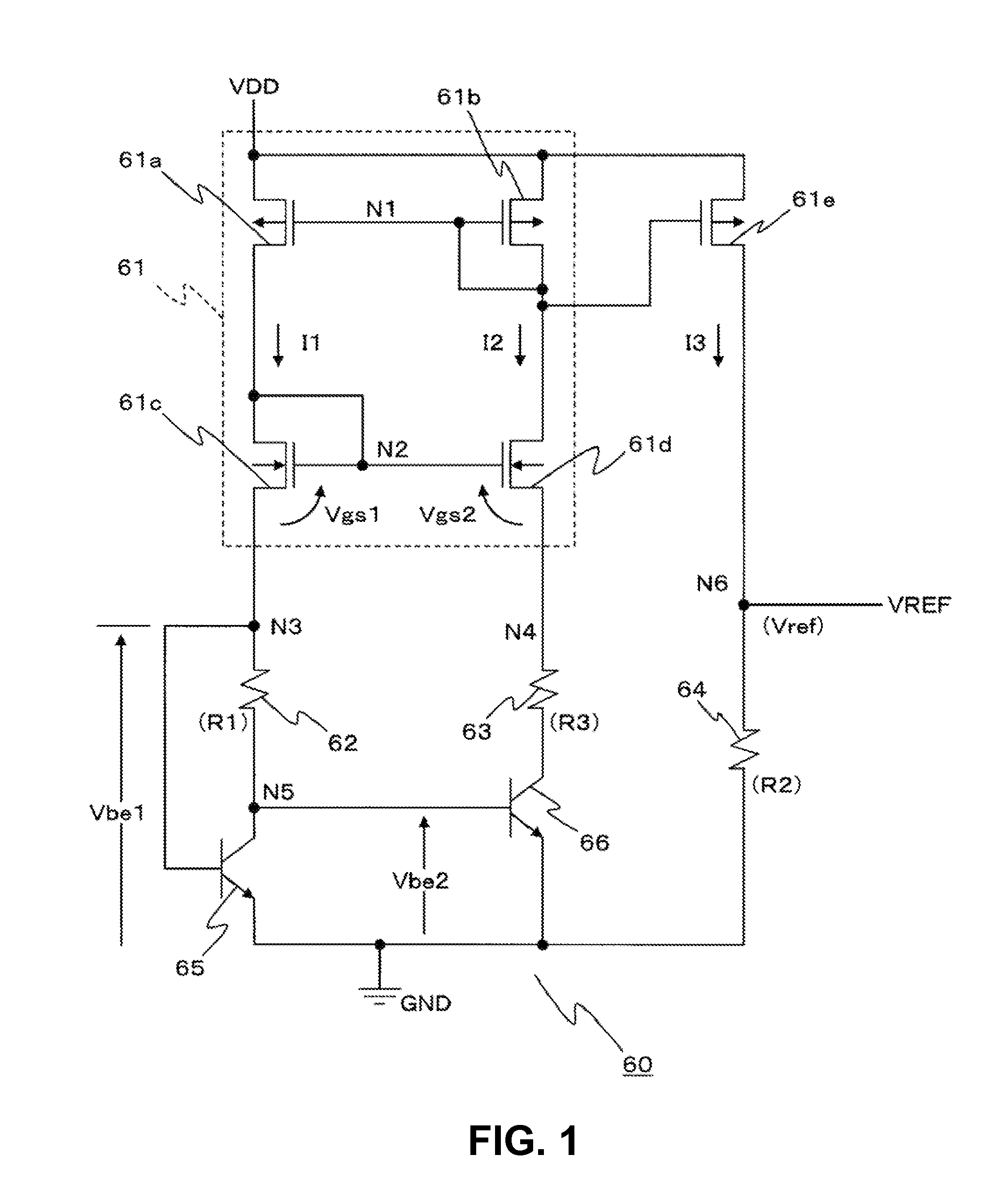
[0142]FIG. 11 is a circuit diagram showing a configuration of the reference voltage generation circuit 60C according to the third embodiment of the present invention. Components of the reference voltage generation circuit 60C similar to those of the reference voltage generation circuit 60 shown in FIG. 1 are designated with the same reference numerals.
[0143]In the second embodiment, the reference voltage generation circuit 60C is configured such that...
PUM
 Abstract
Description
Claims
Application Information


