
Critical-path circuit for performance monitoring

Inactive Publication Date: 2011-11-03
AVAGO TECH WIRELESS IP SINGAPORE PTE
View PDF11 Cites 19 Cited by
  • Summary
  • Abstract
  • Description
  • Claims
  • Application Information

AI Technical Summary

Benefits of technology

[0012]Problems in the prior art are addressed in accordance with the principles of the present invention by an improved timing-monitor circuit placed in a region near a critical path to be monitored in an integrated circuit.
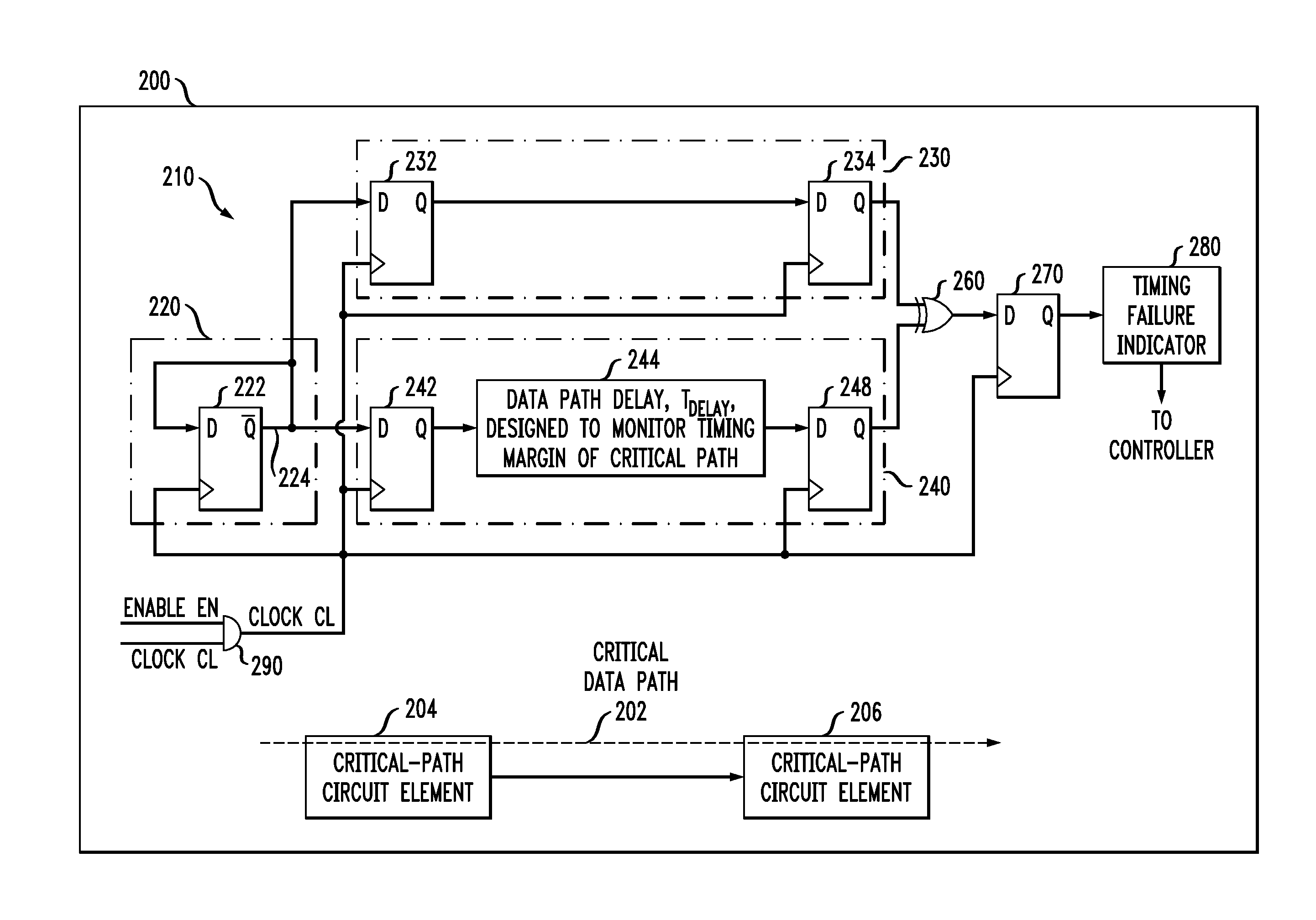
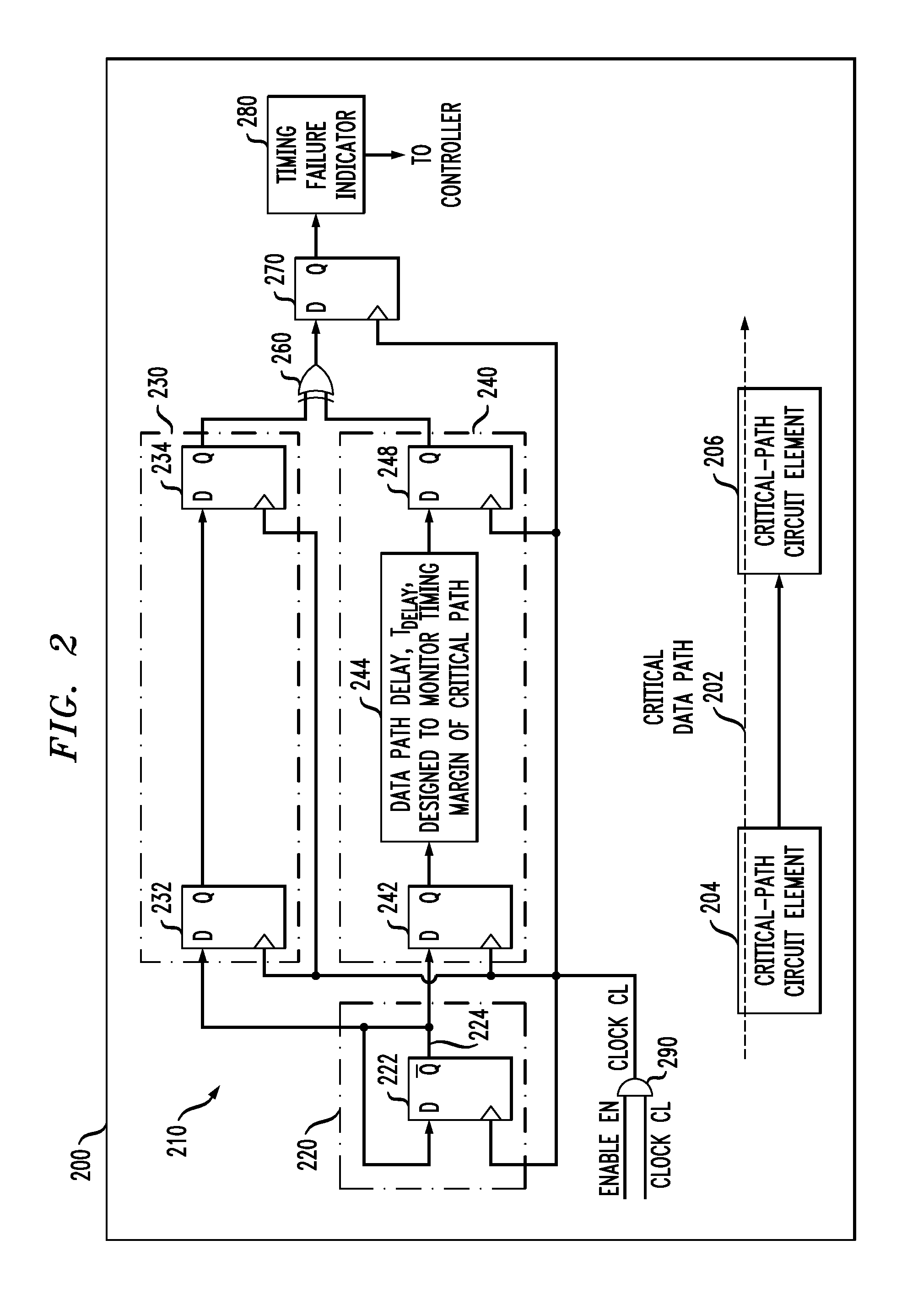
[0013]Thus, in one embodiment, the present invention is an integrated circuit having a monitor circuit for monitoring timing in a critical path in the integrated circuit. The critical path has a target timing margin. The monitor circuit includes a first shift register having an input and an output and having a delay circuit that applies a delay value to a received signal. The monitor circuit further includes a second shift register having an input and an output, wherein the inputs of the first and second shift registers are connected together to form a signal input node capable of receiving an input signal. The monitor circuit also includes a logic circuit having an output and at least two inputs, each input connected to a corresponding one of the outputs of the first and second shift registers. The output of the logic circuit indicates whether the target timing margin is satisfied or not satisfied.
[0014]In another embodiment, the present invention is an apparatus fo

Problems solved by technology

As the integrated circuit ages over time, the actual timing of the signals in each critical path tends to degrade.
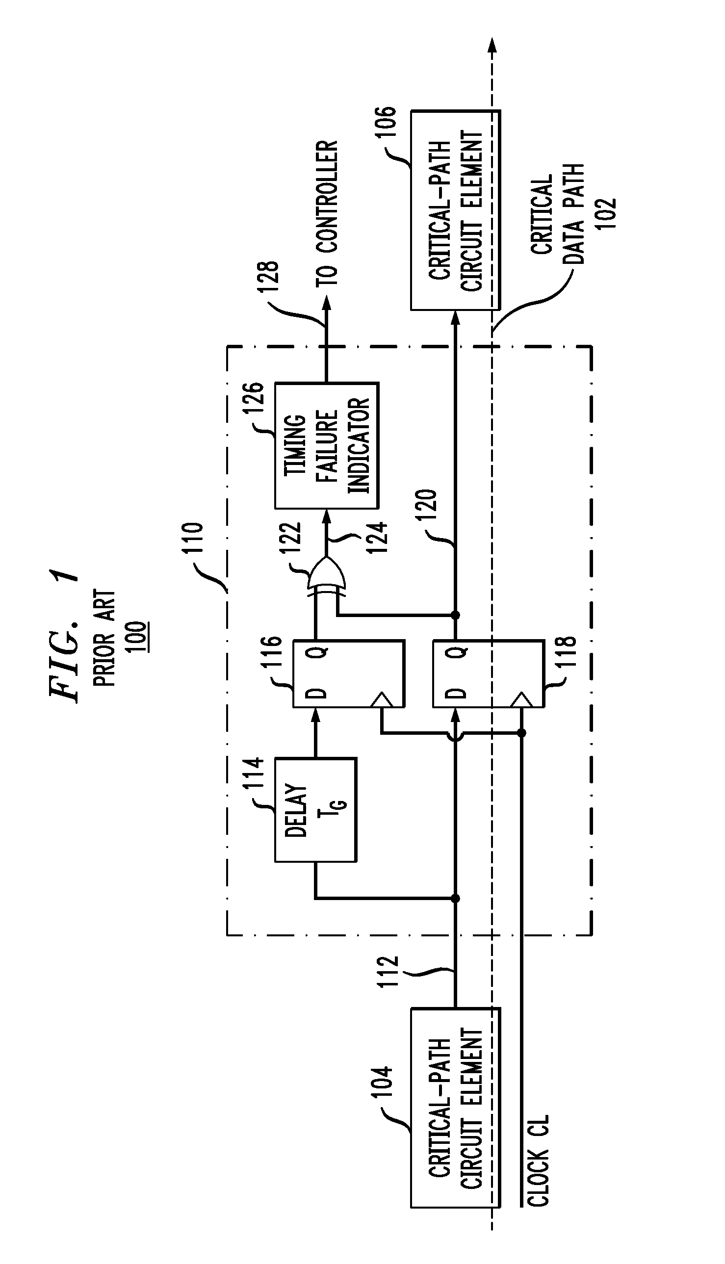
When a timing-monitor circuit determines that the actual timing margin of a signal in a critical path is less than the target timing margin, one may anticipate that a circuit failure is likely to occur, and the integrated circuit may take steps to self-correct, e.g., by adjusting the clock frequency, the voltage supply, or even the body bias voltage of the transistors in the integrated circuit.
As such, a timing failure will be more likely to occur, e.g., as the circuit continues to age.
Under certain circumstances, however, timing-monitor circuit 110 may give an erroneous indication that the timing for critical path 102 is satisfied, even though a setup violation may occur.
Third, timing-monitor circuits are typically added to an integrated circuit only after the physical design and static timing analysis (including the identification of critical paths) for the integrated circuit have been completed.

Method used


Image

  • Critical-path circuit for performance monitoring
  • Critical-path circuit for performance monitoring
  • Critical-path circuit for performance monitoring

Examples


case 1

Timing Margin Met With No Excess Margin

[0042]FIG. 5 illustrates the timing for Case 1, in which the target timing margin is met with no excess margin. In Case 1, the design value for the sum of the delays (i) from the clock CL to output Q of flip-flop 342, (ii) through gross-delay element 344, and (iii) through fine-delay detector 346 (e.g., the time for signal TRIN to travel to signal TROUT) is selected to be equal to about one clock period (i.e., the target timing margin is assumed to be minimal, such that little or no slack exists).

[0043]A data logic value 1 is latched into flip-flops 332 and 342 in FIG. 3 on the first rising edge of the clock CL, as shown at time t1 in the timing diagram in FIG. 5. Accordingly, the Q outputs of flip-flops 332 and 342 transition from a logic value 0 to a logic value 1.

[0044]Just before the second rising edge of the clock CL at time t2 in FIG. 5, by design, the 0-to-1 transition will be observed across the entire gross-delay element 344 and the ou...

case 2

Timing Margin Met With Significant Excess Margin

[0046]FIG. 6 illustrates the timing for Case 2, in which the target timing margin is met with significant excess margin. In Case 2, as in Case 1, the design value for the sum of the delays (i) from the clock CL to output Q of flip-flop 342, (ii) through gross-delay element 344, and (iii) through fine-delay detector 346 is selected to be equal to about one clock period (i.e., the target timing margin is assumed to be minimal, such that little or no slack exists). In Case 2, however, it is assumed that a combination of clock-distribution slow down and / or data-path speed up over time has resulted in the 0-to-1 transition occurring farther down the delay line than originally designed.

[0047]Initially, a logic value 1 is clocked into flip-flops 332 and 342 on the first rising edge of clock CL, as shown at time t1 on the timing diagram in FIG. 6. Accordingly, the Q outputs of flip-flops 332 and 342 transition from a logic value 0 to a logic v...

case 3

Not Met With Setup Violation

[0049]FIG. 7 illustrates Case 3, in which the target timing margin is not met, and a setup violation is detected. In Case 3, as in Cases 1 and 2, the initial value for the sum of the delays (i) from the clock CL to output Q of flip-flop 342, (ii) through gross-delay element 344, and (iii) through fine-delay detector 346 is selected to be equal to about one clock period (i.e., the target timing margin is assumed to be minimal, such that little or no slack exists). In Case 3, however, a combination of clock-distribution speed-up and / or data-path slow-down over time has resulted in the 0-to-1 transition occurring so far up the delay line that the target timing margin is exceeded, and a setup violation occurs.

[0050]In Case 3, at time t1 in FIG. 7, a logic value 1 is clocked into flip-flops 332 and 342 on the first rising edge of clock CL. Accordingly, the Q outputs of flip-flops 332 and 342 transition from a logic value 0 to a logic value 1. Just before the s...


PUM


Abstract

An integrated circuit having a monitor circuit for monitoring timing in a critical path having a target timing margin is disclosed. The monitor circuit has two shift registers, one of which includes a delay element that applies a delay value to a received signal. The inputs to the two shift registers form a signal input node capable of receiving an input signal. The monitor circuit also has a logic gate having an output and at least two inputs, each input connected to a corresponding one of the outputs of the two shift registers. The output of the logic gate indicates whether the target timing margin is satisfied or not satisfied.

Description

BACKGROUND OF THE INVENTION[0001]1. Field of the Invention[0002]The present invention relates to digital integrated circuits, and, in particular, to timing-error detection in digital circuits.[0003]2. Description of the Related Art[0004]In recent years, circuit designers have investigated various approaches for predicting failures in integrated circuits (ICs). One such approach is known as critical-path performance monitoring. In conventional critical-path performance monitoring, a circuit designer identifies one or more signal paths that are deemed to be critical for the proper operation of an integrated circuit (known as “critical paths” or “critical data paths”), usually a path having a maximum delay. For a given circuit element within the critical path, the designer further identifies a target timing margin, i.e., a period of time before which a data signal transition should arrive at the circuit element, relative to a clock signal transition. A timing-monitor circuit (or “aging...

Claims


Application Information

Patent Timeline
IPC IPC(8): H03K19/00
CPCG01R31/31858H03K19/00H03K5/135H03K5/19
Inventor CHLIPALA, JAMES D.MARTIN, RICHARD P.MUSCAVAGE, RICHARDSEGAN, SCOTT A.
Owner AVAGO TECH WIRELESS IP SINGAPORE PTE
Learn More