Printed circuit board with low propagation skew between signal traces

a technology of printed circuit boards and signal traces, applied in the direction of printed circuit aspects, printed circuit manufacturing, conductive pattern formation, etc., can solve the problem that circuit devices that depend on signals to operate incorrectly, data rates in pcbs are skew between signals, and skew can still be a problem in pcbs, so as to achieve the effect of minimizing skew

Active Publication Date: 2011-11-10
ORACLE INT CORP
View PDF12 Cites 11 Cited by
  • Summary
  • Abstract
  • Description
  • Claims
  • Application Information

AI Technical Summary

Benefits of technology

[0008]The described embodiments provide a printed circuit board (PCB) configured to minimize skew between signals propagated on two parallel signal trace portions. The PCB comprises a laminate layer, which includes a fiberglass weave and a plastic resin deposited on a first face and second face of the fiberglass weave to form a first face and second face of the laminate layer. The fiberglass weave includes a first set of fiberglass bundles in a first orientation interwoven with a second set of fiberglass bundles in a second orientation.

Problems solved by technology

One common problem with communicating signals at high data rates in PCBs is skew between the signals.
However, because the propagation time of signals traveling in the interconnect pair can be different due to physical differences in each signal trace in the interconnect pair, the signals can experience different propagation times (i.e., propagation skew), which can cause the circuit devices that depend on the signals to operate incorrectly.
Because many PCBs include two or more layers in which signal traces are routed, one of the main sources for propagation skew is electromagnetic interference between signals on neighboring trace layers of a PCB.
Unfortunately, even with the embedded fiberglass weave, skew can still be a problem in PCBs.
This problem still arises because the dielectric constant can vary across a trace layer of a PCB when some points of the trace layer are near a resin-rich portion of the PCB, while other points are near a fiberglass-rich portion of the PCB.
Even these small variations in the laminate layer's dielectric constant can cause sufficient skew between signals to cause errors in high-performance circuit devices.

Method used


Image

  • Printed circuit board with low propagation skew between signal traces
  • Printed circuit board with low propagation skew between signal traces
  • Printed circuit board with low propagation skew between signal traces

Examples


Embodiment Construction

[0026]The following description is presented to enable any person skilled in the art to make and use the embodiments, and is provided in the context of a particular application and its requirements. Various modifications to the disclosed embodiments will be readily apparent to those skilled in the art, and the general principles defined herein may be applied to other embodiments and applications without departing from the spirit and scope of the present disclosure. Thus, the present invention is not limited to the embodiments shown, but is to be accorded the widest scope consistent with the principles and features disclosed herein.

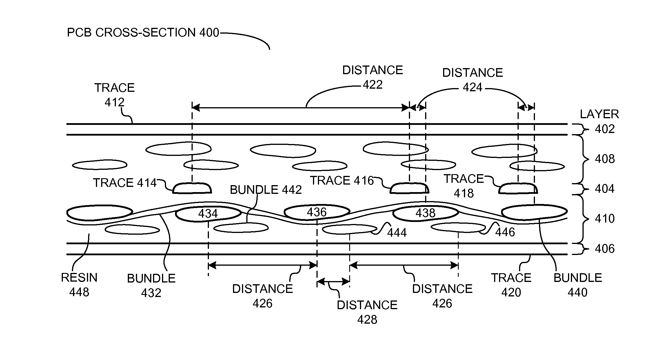
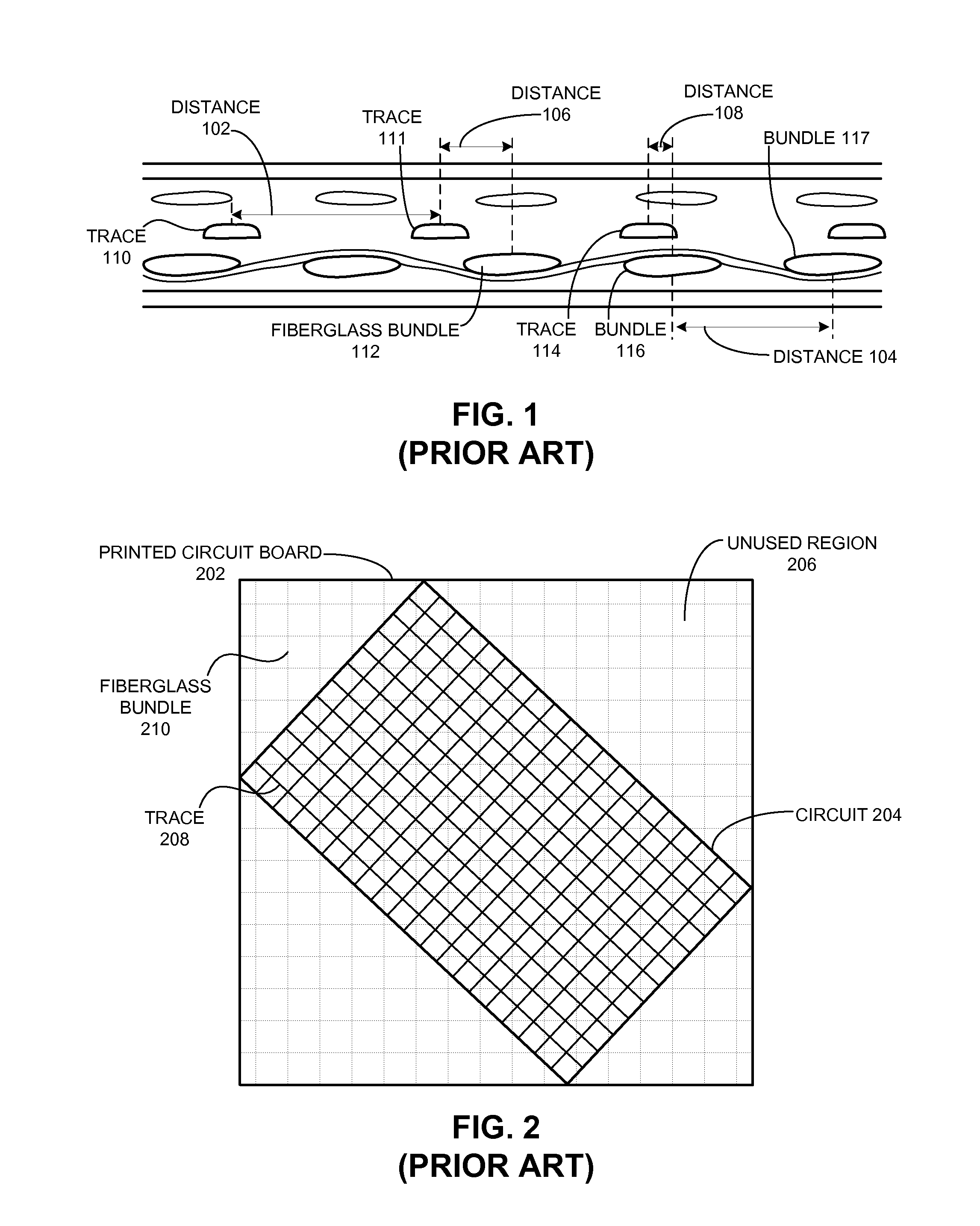
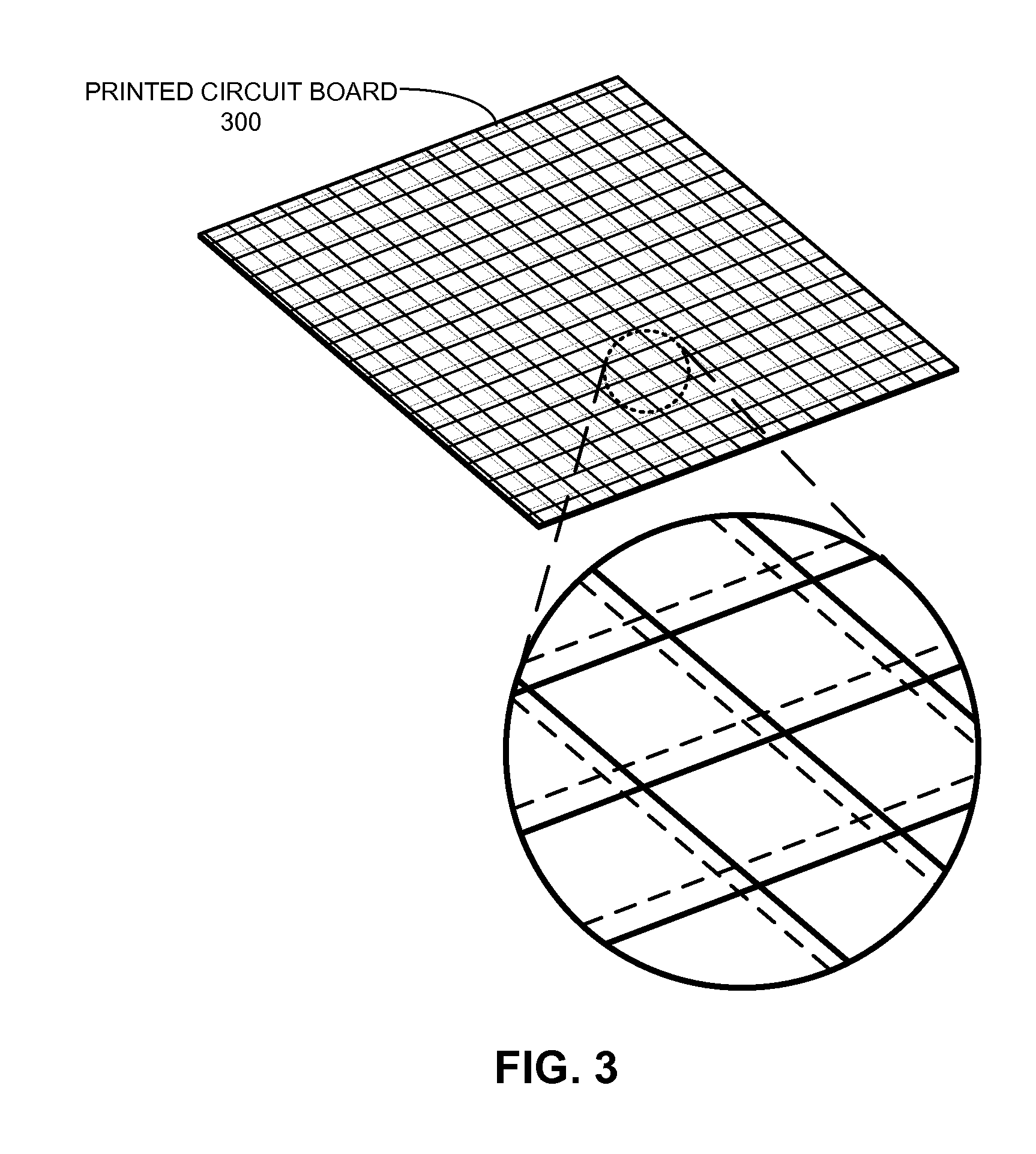
[0027]Typical printed circuit boards (PCBs) include a fiberglass weave within a laminate layer to electrically insulate communication signals that propagate across neighboring trace layers (i.e., to reduce capacitive coupling between the signal traces in the neighboring trace layers). However, as the performance of electronic components increases, even min...


PUM

PropertyMeasurementUnit
average separation distanceaaaaaaaaaa
dielectric constantaaaaaaaaaa

Abstract

A printed circuit board (PCB) is configured to minimize skew between two parallel signal trace portions. The PCB comprises a laminate layer, which includes a fiberglass weave and includes a plastic resin deposited on each face of the fiberglass weave to form a first face and second face of the laminate layer. The fiberglass weave comprises a first set of fiberglass bundles in a first orientation interwoven with a second set of fiberglass bundles in a second orientation. Moreover, the PCB comprises trace a layer that is coupled to the first face of the laminate layer, and includes two or more signal traces. Two parallel trace portions of the two or more signal traces are configured to have a matching orientation and separation distance to a neighboring fiberglass bundle of the fiberglass weave, thereby ensuring that the two parallel trace portions encounter matching dielectric constants from the laminate layer.

Description

BACKGROUND[0001]1. Field[0002]This disclosure is related to printed circuit boards (PCBs). More specifically, this disclosure relates to a printed circuit board which is configured to minimize skew between parallel signal traces.[0003]2. Related Art[0004]Advances in fabrication technologies continue to increase the performance and maximum throughput of circuit devices. However, enabling the circuit devices to maintain high throughput generally requires that circuit devices communicate with one another at high data rates. The requirement for high data-rate communication between circuit devices is increasing demand for printed circuit boards (PCBs) with interconnects (i.e., signal wires / traces fabricated in the PCB) that can carry communication signals between the circuit devices at high data rates.[0005]One common problem with communicating signals at high data rates in PCBs is skew between the signals. More specifically, many PCBs include pairs of interconnections that simultaneousl...

Claims


Application Information

Patent Timeline
Patent Type & Authority Applications(United States)
IPC IPC(8): H05K1/00H05K3/10
CPCH05K1/0245H05K1/0248Y10T29/49124H05K2201/029H05K1/0366
Inventor FREDA, MICHAEL C.WILLIAMS, RICKI D.
Owner ORACLE INT CORP
Why Eureka
Try Eureka