Semiconductor unit and semiconductor apparatus using same

Inactive Publication Date: 2011-11-17
FUJI ELECTRIC CO LTD
View PDF6 Cites 14 Cited by
  • Summary
  • Abstract
  • Description
  • Claims
  • Application Information

AI Technical Summary

Benefits of technology

[0018]In view of the above-described problems, it is an object of embodiments of the present invention to solve the above-problems and provide a semiconductor u

Problems solved by technology

This requirement for ensuring the heat transfer area raises a problem of increase in a module size.
This requirement for ensuring the distance raises a problem of increase in a module size.
In order to ensure sufficient magnitude of electric current capacity, the number of aluminum wires needs to be increased, which however, increases the number of wiring places of the wires and the

Method used


Image

  • Semiconductor unit and semiconductor apparatus using same
  • Semiconductor unit and semiconductor apparatus using same
  • Semiconductor unit and semiconductor apparatus using same

Examples


example 1

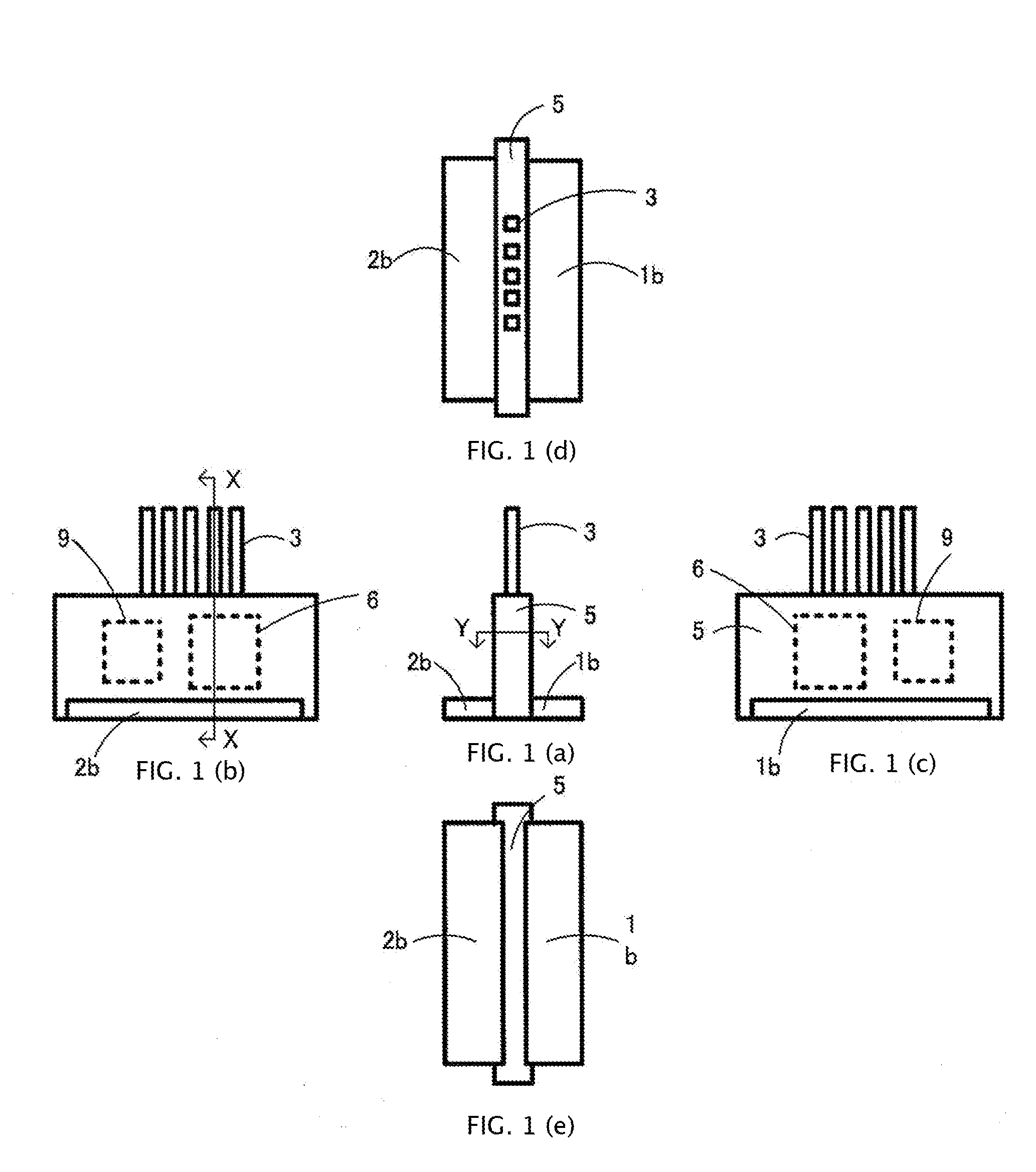
[0058]FIGS. 1(a) through 1(e) are external views of a semiconductor unit 100 of Example 1 according to embodiments of the present invention, in which FIG. 1(a) is a front view, FIG. 1(b) is a left side view, FIG. 1(c) is a right side view, FIG. 1(d) is a top plan view, and FIG. 1(e) is a bottom plan view.

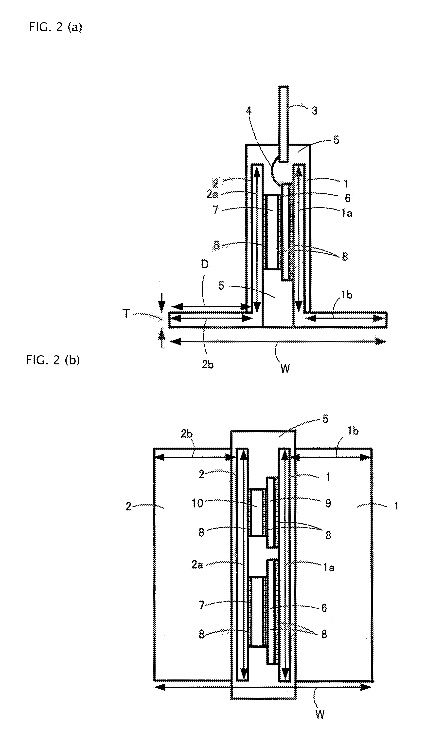
[0059]FIGS. 2(a) and 2(b) are sectional views of the semiconductor unit 100 of FIGS. 1(a) through 1(e), in which FIG. 2(a) is a sectional view cut along the line X-X in FIG. 1(b) and FIG. 2(b) is a sectional view cut along the line Y-Y in FIG. 1(a).

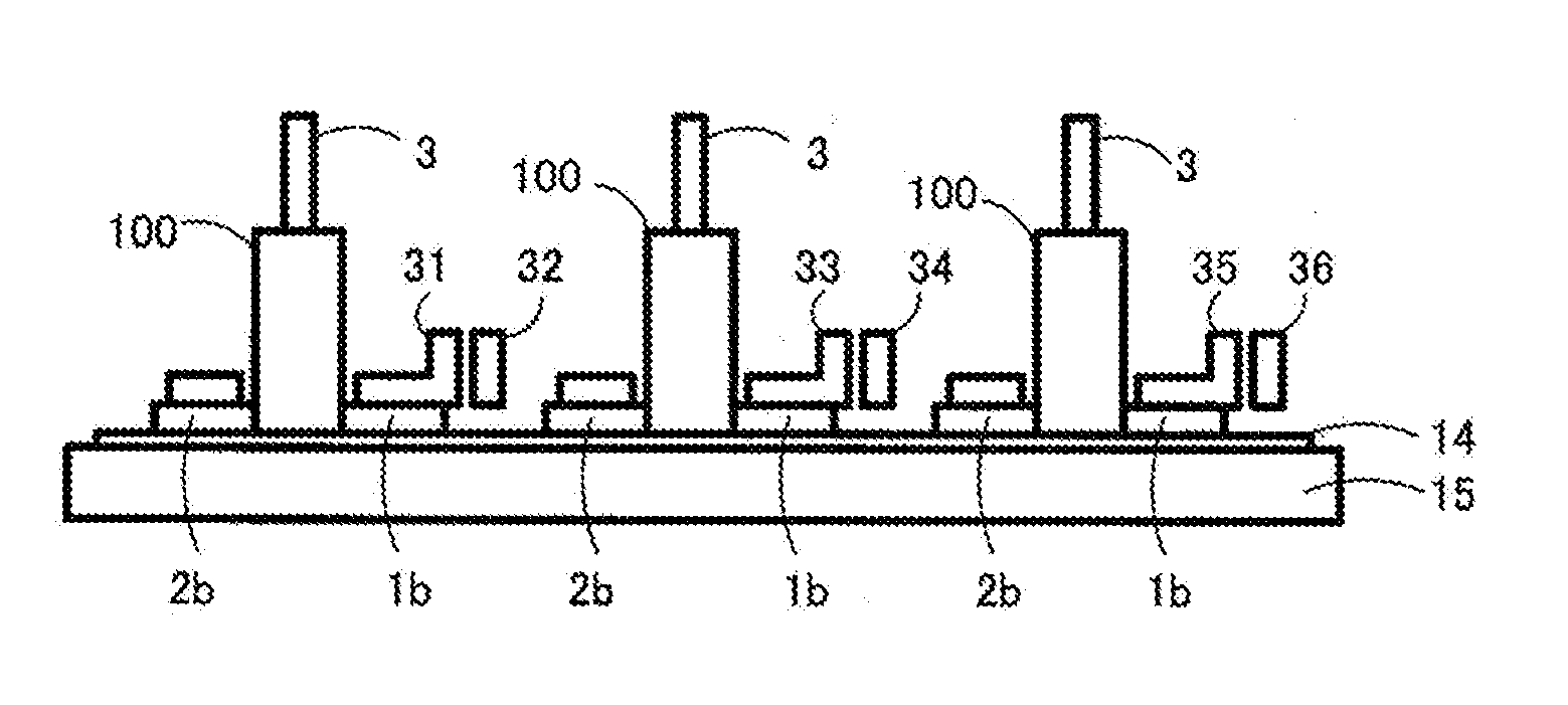
[0060]This semiconductor unit 100 comprises a pair of electrically conductive plates in the shape of the letter L. The electrically conductive plate consists of a flat body portion and a leg portion that is continuous and perpendicular to the flat body portion. An undepicted collector electrode of an IGBT chip 6 is soldered to an L-shaped electrically conductive plate 1 for collector with a solder 8. An L-shaped electrically conductive pl...

example 2

[0082]FIG. 4 is a sectional view of an essential part of a semiconductor apparatus of Example 2 according to the present invention. This example contains one unit of the semiconductor unit shown in FIGS. 1(a) through 1(e).

[0083]This semiconductor apparatus 200 comprises: a semiconductor unit 100 described previously, a cooling plate 15 fixed through an insulation layer 14 with the bottom surfaces of the leg portions 1b and 2b of the semiconductor unit 100 (the leg portion 1b of the L-shaped electrically conductive plate 1 for collector and the leg portion 2b of the L-shaped electrically conductive plate 2 for emitter); a lead out terminal 17 for collector and a lead out terminal 18 for emitter connected to the leg portions 1b and 2b; a casing 20 containing the semiconductor unit 100 and the lead out terminals 17, 18 and connected to the cooling plate 15; and gel 21 (insulation material, for example, silicone gel) put in the casing 20. The control terminals 3 and the lead out termina...

example 3

[0093]FIG. 6 is a sectional view of an essential part of a semiconductor apparatus of Example 3 according to the invention. This semiconductor apparatus 300 is different from the semiconductor apparatus 200 of FIG. 4 in that a drive circuit board 22 is disposed above the casing 20. The drive circuit board 22 has circuit components mounted thereon to control and protect the IGBT chip 6.

[0094]The control terminals 3 lead out from the semiconductor unit 100 are joined to a circuit pattern (not shown in the figure) on the drive circuit board 22.


PUM


Abstract

A semiconductor unit of certain aspects of the invention includes electrically conductive plates in the shape of the letter L, each consisting of a horizontally disposed leg portion and a vertically disposed flat body portion that is perpendicular to a cooling plate adhered to the bottom of the semiconductor unit. A pair of the vertically disposed flat body portions sandwiches a semiconductor chip. Owing to this construction, the heat generated in the semiconductor chip can be conducted away through the both surfaces of the chip, thus improving cooling performance. Since the heat is conducted away through the leg portions of the L-shaped electrically conductive plates a projected planar area occupied by the cooling plate required for cooling the semiconductor unit is reduced. Therefore, the size of the semiconductor unit can be reduced.

Description

BACKGROUND OF THE INVENTION[0001]1. Field of the Invention[0002]The present invention relates to a semiconductor unit containing a semiconductor chip, and a semiconductor apparatus using the semiconductor unit.[0003]2. Description of the Related Art[0004]It is known, for example in Japanese Unexamined Patent Application Publication No. 2000-156439 (see FIG. 1), referred to herein as “Patent Document 1,” to construct a semiconductor module, in a package, containing power semiconductor elements such as an IGBT (an insulated gate bipolar transistor), a FWD (a free-wheeling diode) and the like mounted on an insulated substrate.[0005]FIG. 17 is a sectional view of an essential part of a semiconductor module of a first conventional example. FIG. 17 shows a semiconductor module similar to that disclosed in Patent Document 1.[0006]Referring to FIG. 17, an insulated substrate 55 is joined onto a cooling plate 54 with a solder or the like, and an IGBT chip 56 is mounted on the cooling plate 5...

Claims


Application Information

Patent Timeline
IPC IPC(8): H01L29/739H01L23/48
CPCH01L23/367H01L2924/01033H01L24/33H01L24/40H01L24/48H01L24/73H01L24/91H01L25/115H01L2224/32245H01L2224/48091H01L2224/48247H01L2224/73215H01L2224/73265H01L2924/01013H01L2924/01029H01L2924/01047H01L2924/01082H01L2924/13055H01L2924/13091H01L2924/19107H01L24/32H01L2924/1305H01L2224/45124H01L2924/014H01L2924/01074H01L2924/01005H01L2924/01006H01L2924/01023H01L2924/00014H01L2924/00012H01L2924/00H01L2224/40095H01L2224/40225H01L24/45H01L2924/181H01L2224/371H01L2224/84801H01L2224/83801H01L2224/8385H01L2224/8485H01L24/37H01L2224/33181H01L2224/92247H01L2224/2612H01L24/84H01L2924/00015H01L2224/05599H01L2224/73221
Inventor SATO, KENICHIRO
Owner FUJI ELECTRIC CO LTD
Why Eureka
Try Eureka