
Solid-state imaging device and camera

a solid-state imaging and camera technology, applied in the field of solid-state imaging devices and cameras, can solve the problem that the solid-state imaging device b>600/b> cannot suppress the highlight horizontal line noise, and achieve the effect of suppressing power consumption effectively, reducing current fluctuation, and suppressing current fluctuation

Inactive Publication Date: 2011-11-17
PANASONIC CORP
View PDF7 Cites 16 Cited by
  • Summary
  • Abstract
  • Description
  • Claims
  • Application Information

AI Technical Summary

Benefits of technology

[0012]However, the CMOS solid-state imaging device 600 cannot suppress the highlight horizontal line noise when a subject is in a range where amount-of-light is not saturated, that is, when the subject is in a range where amount-of-light is low to middle or the like. This is because gate voltages of the amplifier transistors M311 to M333 inside pixels become higher than the clipped voltage VCG, and thus the clipping transistor does not become ON state.

Problems solved by technology

However, the CMOS solid-state imaging device 600 cannot suppress the highlight horizontal line noise when a subject is in a range where amount-of-light is not saturated, that is, when the subject is in a range where amount-of-light is low to middle or the like.
The variation in the voltage causes a longitudinal line to appear on an image, which is an other image defect.

Method used


Image

  • Solid-state imaging device and camera
  • Solid-state imaging device and camera
  • Solid-state imaging device and camera

Examples


embodiment 1

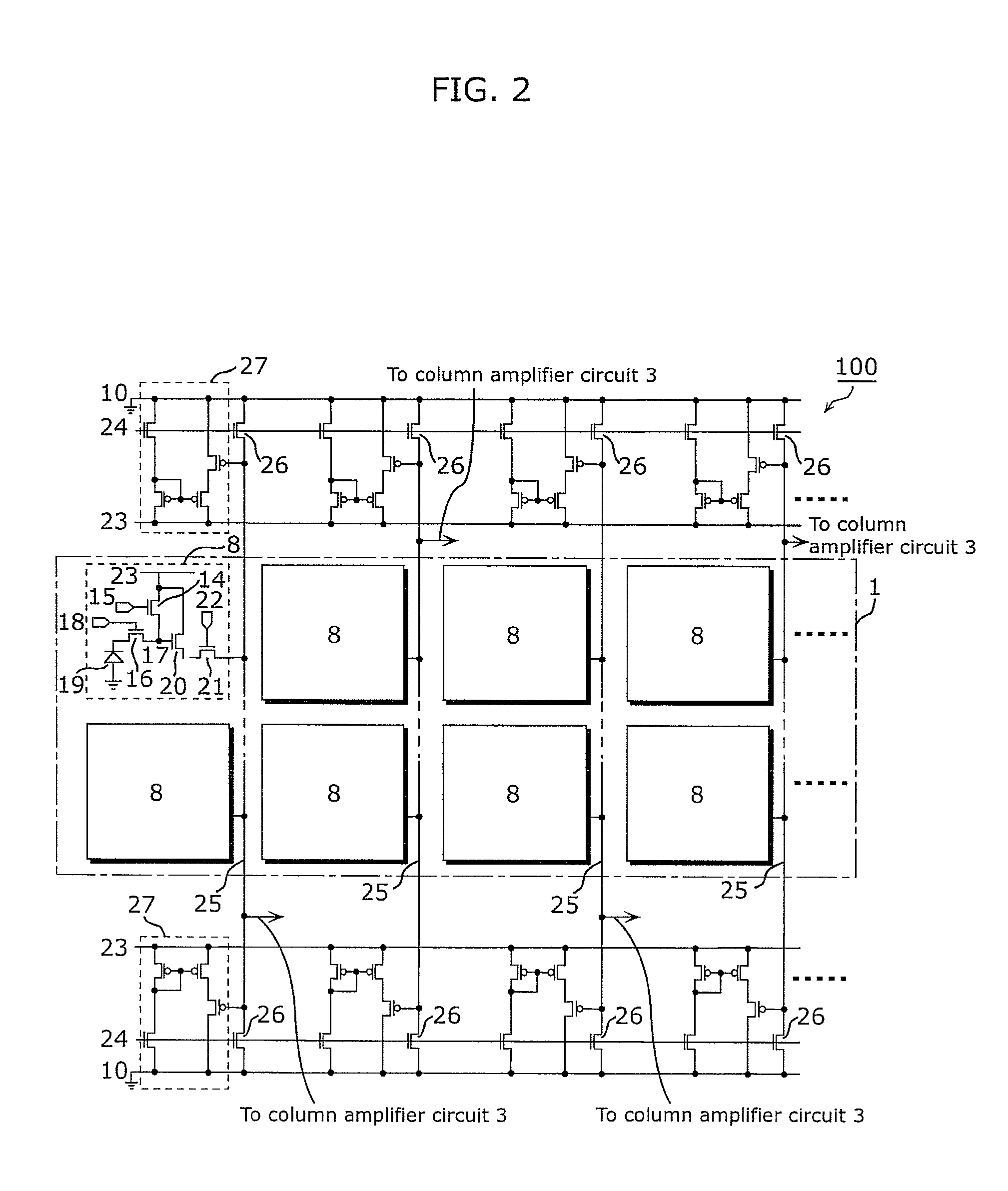
[0050]A solid-state imaging device according to this embodiment includes pixel units arranged in rows and columns. Each of the above described pixel units includes an amplifier element which amplifies a signal voltage, which has been generated by a photoelectric conversion, in response to a flow of an operating current, and outputs an amplified signal voltage to a column signal line which is provided for each of pixel columns. Further, the above described solid-state imaging device includes current correction units each of which is provided for a corresponding one of the pixel columns and configured to cause a correction current to flow between a power supply line and a grounding line, the correction current fluctuating in an opposite direction to a fluctuation of the operating current flowing into the grounding line from the power supply line via the amplifier element. With this, regardless of the amount of incident light, it is possible to reduce a highlight horizontal line noise....

embodiment 2

[0099]Next, a solid-state imaging device according to Embodiment 2 of the present invention is described with reference to a drawing.

[0100]FIG. 6 is a circuit configuration diagram showing a pixel array and a pixel source follower circuit of a solid-state imaging device according to Embodiment 2 of the present invention. The pixel array 1 is composed of pixel units 8 arranged in rows and columns. A solid-state imaging device 200 further includes column signal lines 25. The column signal lines 25 are provided for each of the columns arranged in rows and columns.

[0101]The solid-state imaging device 200 according to Embodiment 2 shown in FIG. 6 is the same as the solid-state imaging device 100 according to Embodiment 1 shown in FIG. 2 except for a configuration of a current correction circuit 27. The description of points common to the solid-state imaging device 100 shown in FIG. 2 is omitted, and the following describes only different points.

[0102]In the solid-state imaging device 200...

embodiment 3

[0104]Next, a solid-state imaging device according to Embodiment 3 of the present invention and a camera which includes the solid-state imaging device are described with reference to drawings.

[0105]FIG. 7 is a functional block diagram showing a camera according to Embodiment 3 of the present invention. The camera shown in FIG. 7 includes a solid-state imaging device 41, a noise canceling circuit 42, a gain amplifier 43, an analog-to-digital converter (ADC) 44, and a digital signal processor (DSP) 45.

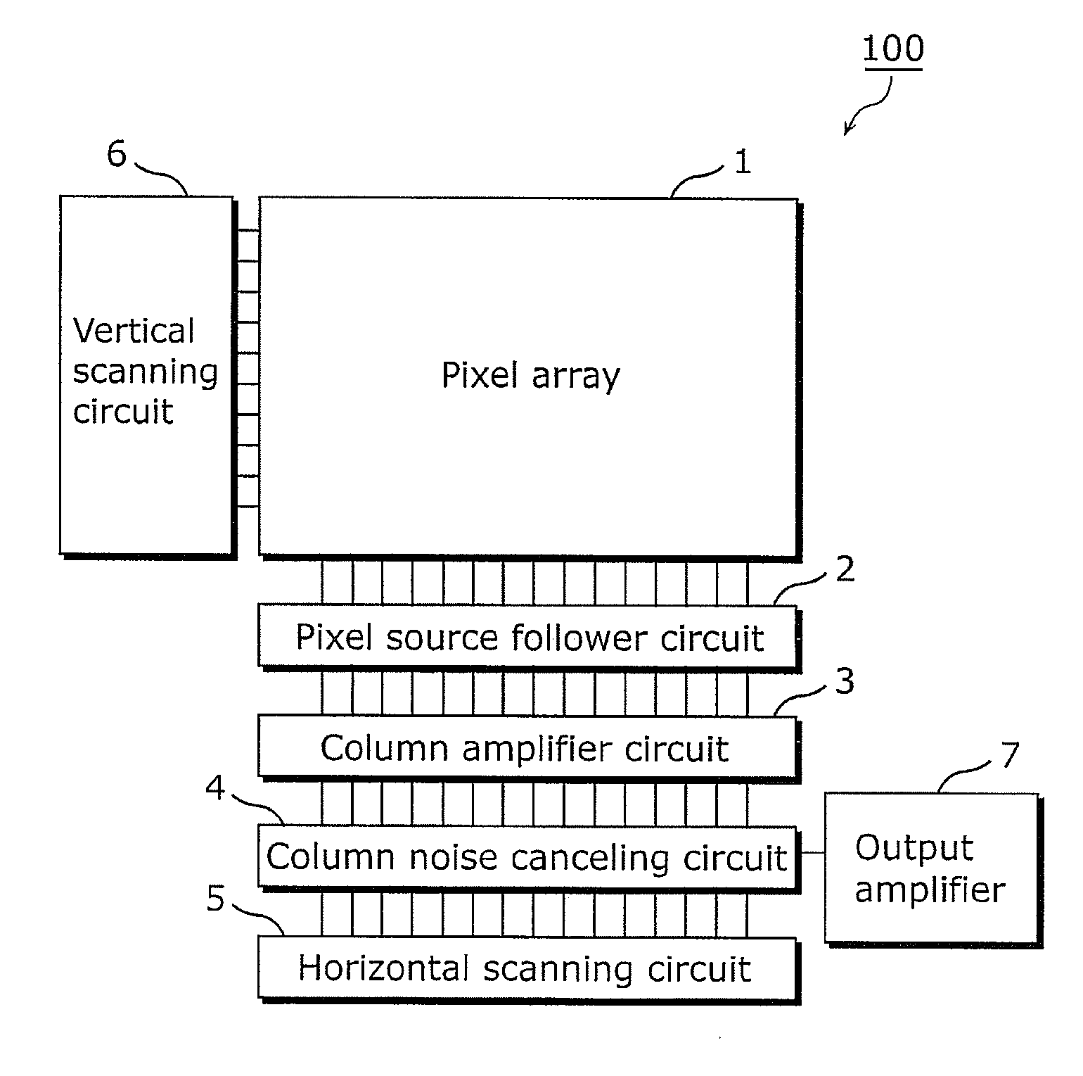
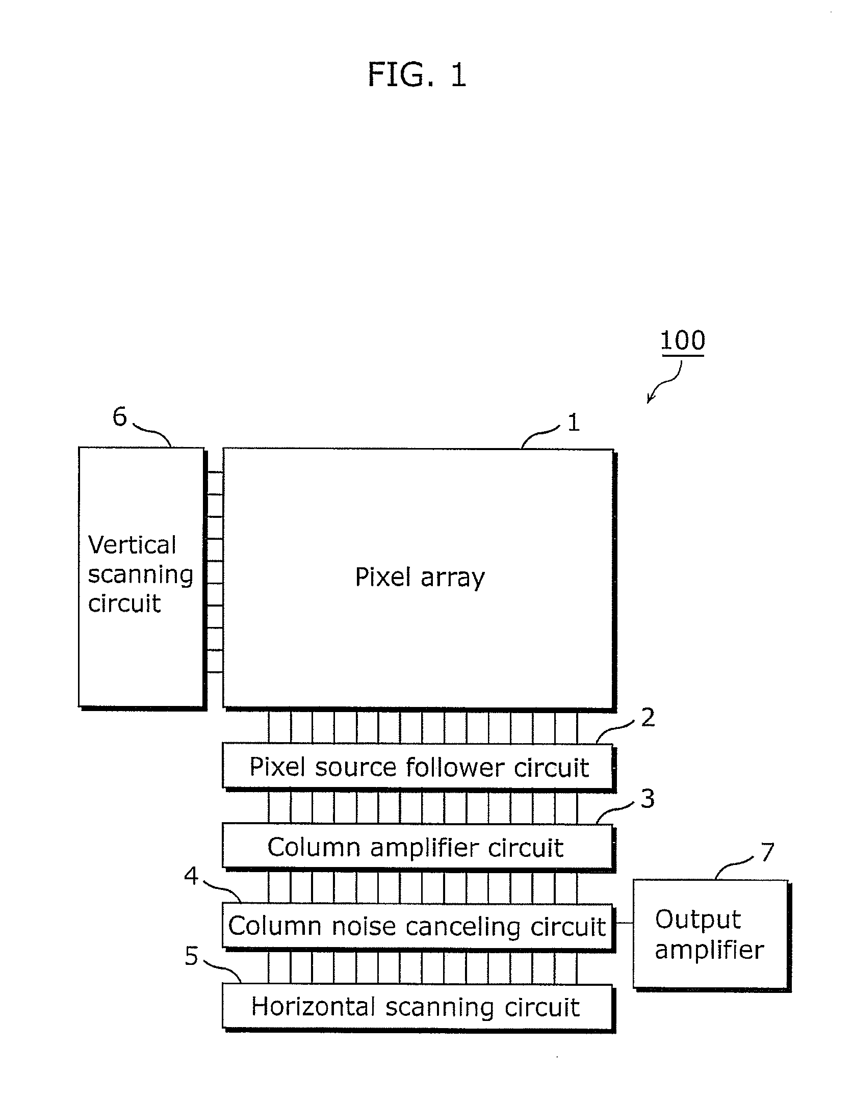
[0106]The solid-state imaging device 41 is a solid-state imaging device according to the present invention, and has the same configuration as shown in FIG. 1. Furthermore, the solid-state imaging device 41 is the same as the solid-state imaging device 100 shown in FIG. 2 and the solid-state imaging device 200 shown in FIG. 6, except for a configuration of a current correction circuit. The configuration and an operation of the current correction circuit will be described later. As shown i...


PUM


Abstract

The solid-state imaging device includes a plurality of pixel units arranged in rows and columns. Each of the pixel units includes: a photodiode that generates a signal voltage corresponding to an intensity of light received; and an amplifier transistor which amplifies the signal voltage in response to a flow of an operating current, and outputs the amplified signal voltage to a column signal line that is provided for each of pixel columns. The solid-state imaging device includes current correction circuits each of which is provided for a corresponding one of the pixel columns and causes a correction current to flow between a power supply line and a grounding line. The correction current fluctuates in an opposite direction to a fluctuation of the operating current flowing into the grounding line from the power supply line via the amplifier element.

Description

CROSS REFERENCE TO RELATED APPLICATION[0001]This is a continuation application of PCT application No. PCT / JP2009 / 007234 filed on Dec. 25, 2009, designating the United States of America.BACKGROUND OF THE INVENTION[0002](1) Field of the Invention[0003]The present invention relates to solid-state imaging devices and cameras, and in particular to a solid-state imaging device and a camera which can capture a defect-free high quality image, especially when capturing a subject of high luminance.[0004](2) Description of the Related Art[0005]A Metal Oxide Semiconductor (MOS) image sensor accumulates, in a gate electrode of a MOS transistor, a photocarrier generated by a photodiode and, according to a drive timing given by a scanning circuit, performs charge amplification on a change of a potential of the gate electrode, and outputs the amplified potential change to an outputting unit. FIG. 10 is a block diagram showing a configuration of a conventional Complementary Metal Oxide Semiconductor...

Claims


Application Information

Patent Timeline
IPC IPC(8): H04N5/335H01L27/146H04N5/365H04N5/374H04N5/3745
CPCH04N5/3745H01L27/14609H04N25/77H04N25/78
Inventor NAKAGAWA, TAKUMAKUBO, HIROSHI
Owner PANASONIC CORP
Learn More