Current sensor

a current sensor and sensor technology, applied in the field of current sensor, can solve the problems of reducing the accuracy with which the electric current is detected, and causing offset, so as to prevent the reduction of the current detection accuracy

Inactive Publication Date: 2011-11-24
DENSO CORP
View PDF4 Cites 37 Cited by
  • Summary
  • Abstract
  • Description
  • Claims
  • Application Information

AI Technical Summary

Benefits of technology

[0005]In view of the above, it is an object of the present invention to provide a current sensor for preventing a reduction in current detection accuracy due to an offset in an output voltage of a sensor chip.

Problems solved by technology

The offset reduces the accuracy with which the electric current is detected.
Also, such an offset can occur due to the mismatch in resistance between the magnetoresistive elements of a bridge circuit and due to age deterioration of the sensor chip and the bias magnet.

Method used


Image

  • Current sensor
  • Current sensor
  • Current sensor

Examples


first embodiment

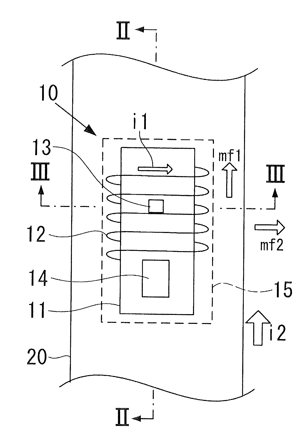
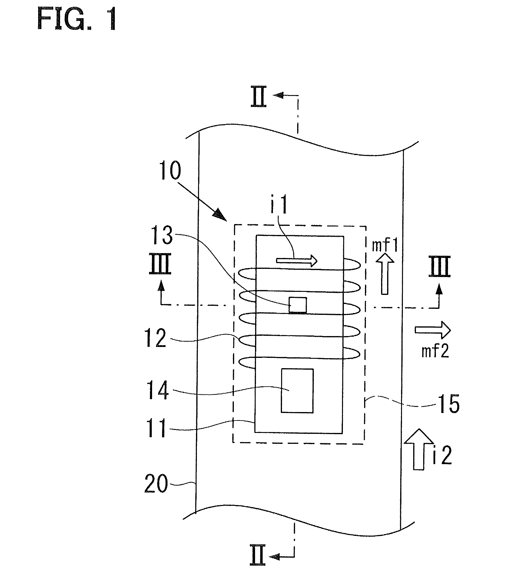
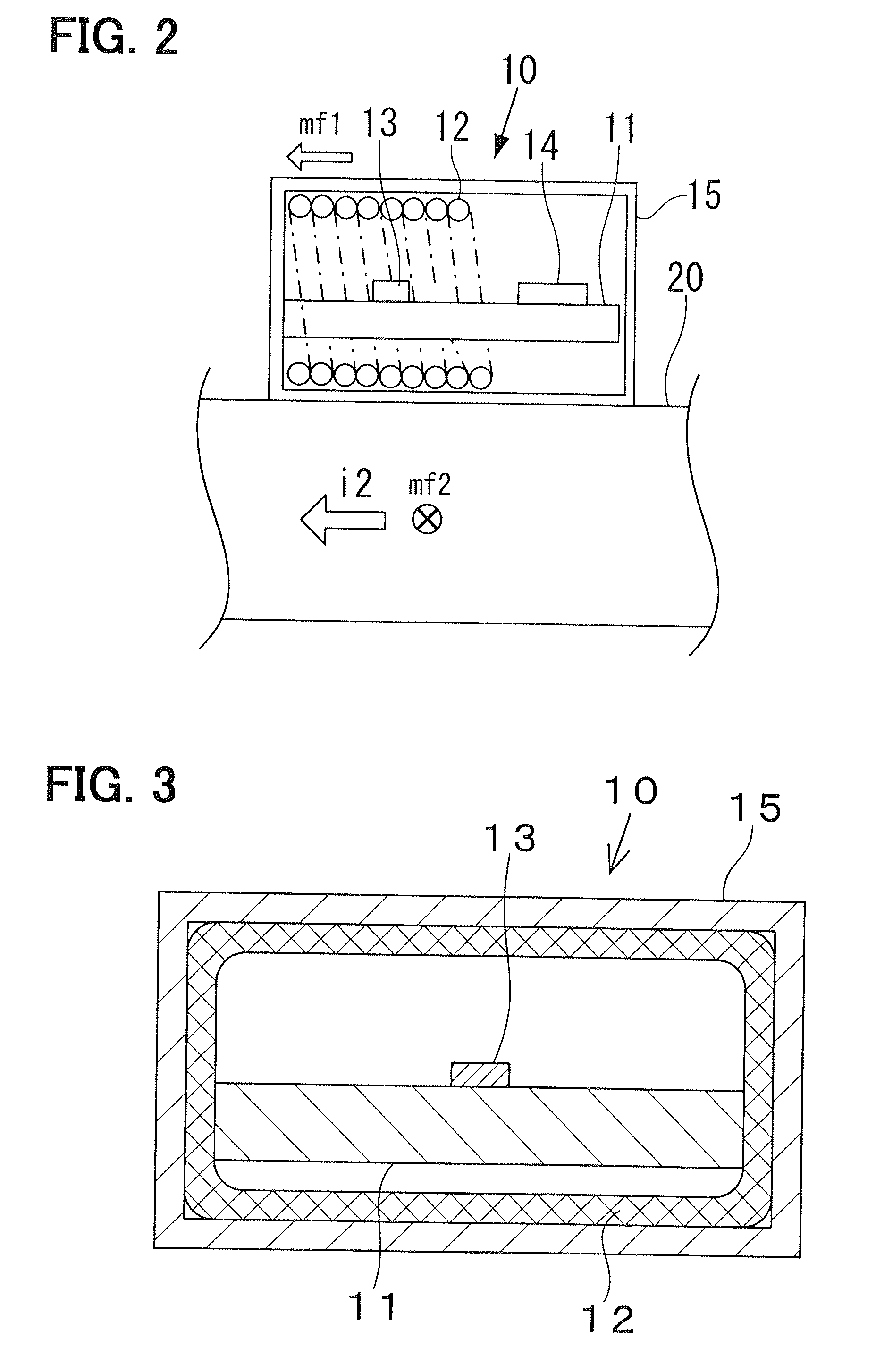
[0024]A current sensor 10 according to a first embodiment of the present invention is described below with reference to FIGS. 1-5. FIG. 1 is a diagram illustrating a plan view of the current sensor 10. FIG. 2 is a diagram illustrating a cross-sectional view taken along the line II-II in FIG. 1. FIG. 3 is a diagram illustrating a cross-sectional view taken along the line in FIG. 1. FIG. 4A is a diagram illustrating a positional relationship between a sensor chip 13 and a coil 12 of the current sensor 10, and FIG. 4B is a diagram illustrating a vertical cross-sectional view of the sensor chip 13. FIG. 5 is a diagram illustrating a layout of magnetoresistive elements Ra-Rd and a magnetic vector.

[0025]As shown in FIGS. 1 and 2, the current sensor 10 includes a substrate 11, a coil 12, the sensor chip 13, a circuit chip 14, and a casing 15. The sensor chip 13 and the circuit chip 14 are attached to a front surface of the substrate 11. As shown in FIG. 3, the substrate 11 and the coil 12 ...

second embodiment

[0053]A current sensor 10 according to a second embodiment of the present invention is described below with reference to FIGS. 13 and 14. FIG. 13 is a diagram illustrating a plan view of the current sensor 10. FIG. 14 is a diagram illustrating a cross-sectional view taken along the line XIV-XIV in FIG. 13. A difference of the second embodiment from the first embodiment is as follows.

[0054]According to the second embodiment, a core 16 made of a magnetic material is attached to a back surface of the substrate 11 and thus located inside the coil 12. In an example shown in FIGS. 13 and 14, the core 16 has a plate-like shape. Alternatively, the core 16 can have a circular cylindrical shape, for example. The core 16, which is located inside the coil 12, increases the magnetic flux density of the bias magnetic field mf1 generated by the coil 12. Thus, the sensitivity with which the target current i2 is detected can be increased. The core 16 can be located outside the coil 12. The core 16 c...

third embodiment

[0055]A current sensor 10 according to a third embodiment of the present invention is described below with reference to FIG. 15. FIG. 15 is diagram illustrating a perspective view of a sensor chip 13 and a coil 12 of the current sensor 10. A difference of the third embodiment from the preceding embodiments is that the sensor chip 13 is formed by using a wafer level packaging technology.

[0056]Multiple sensor chips 13 are formed into a silicon wafer. Then, another silicon wafer serving as a cap is joined to the silicon wafer so that the sensor chips 13 can be covered with the other silicon wafer. Then, the silicon wafers are divided into individual wafer level packages (WLPs) 17. Specifically, as shown in FIG. 15, the WLP 17 has a main portion 17a and a cap portion 17b. The sensor chip 13 is formed in the main portion 17a, and the cap portion 17b is joined to the main portion 17a so that the sensor chip 13 can be covered with the cap portion 17b. A conductive pattern 18 serving as the...


PUM


Abstract

A current sensor for detecting a first electric current flowing through a current path includes a sensor chip, a coil, a current control circuit, and an output circuit. The sensor chip includes a magnetoresistive element and is adopted to be located near the current path. The coil applies a bias magnetic field to the magnetoresistive element. The current control circuit supplies a second electric current to the coil. The second electric current periodically changes in polarity. The output circuit outputs a difference between a first voltage and a second voltage. The first voltage is generated by the magnetoresistive element, when the second electric current flowing through the coil has a positive polarity. The second voltage is generated by the magnetoresistive element, when the second electric current flowing through the coil has a negative polarity.

Description

CROSS REFERENCE TO RELATED APPLICATION[0001]This application is based on and claims priority to Japanese Patent Application No. 2010-115214 filed on May 19, 2010, the contents of which are incorporated herein by reference.FIELD OF THE INVENTION[0002]The present invention relates to a current sensor for detecting an electric current by using a magnetoresistive element and a bias magnetic field.BACKGROUND OF THE INVENTION[0003]As disclosed in, for example, JP-A-2007-155399, a conventional current sensor includes a sensor chip having a magnetoresistive element, a bias magnet located on both sides of the sensor chip, and a processing unit for calculating the magnitude of an electric current flowing through a current path based on a voltage generated by the sensor chip. A resistance of the magnetoresistive element changes according to a direction of a vector of a combined magnetic field of a magnetic field generated by the bias magnet and a magnetic field generated by the electric curren...

Claims


Application Information

Patent Timeline
Patent Type & Authority Applications(United States)
IPC IPC(8): G01R15/18
CPCG01R15/205
Inventor NOMURA, KOUSUKE
Owner DENSO CORP
Why Eureka
Try Eureka