Ceramic electronic component and method for manufacturing the same

a technology of ceramic electronic components and ceramic coatings, applied in the direction of fixed capacitor details, stacked capacitors, fixed capacitors, etc., can solve the problems of degrading reliability of electronic components and damage to ceramic electronic components, and achieve the effects of effective diffusion, improved adhesion between the underlying electrode layer and the first cu plating film, and improved reliability of ceramic electronic components

Active Publication Date: 2011-12-01
MURATA MFG CO LTD
View PDF18 Cites 37 Cited by
  • Summary
  • Abstract
  • Description
  • Claims
  • Application Information

AI Technical Summary

Benefits of technology

[0010]To overcome the problems described above, preferred embodiments of the present invention provide a highly reliable ceramic electronic component provided with an external electrode including an underlying electrode layer disposed on a ceramic element assembly and a Cu plating film disposed on the underlying electrode layer.

Problems solved by technology

This is because if the reflectance of the external electrode with respect to the laser is low, the laser penetrates to the inside of the ceramic electronic component and, thereby, the ceramic electronic component may be damaged.
Therefore, there is a problem in that the reliability of the electronic component is degraded.

Method used


Image

  • Ceramic electronic component and method for manufacturing the same
  • Ceramic electronic component and method for manufacturing the same
  • Ceramic electronic component and method for manufacturing the same

Examples


example 1

[0110]In the present example, a ceramic electronic component having the same configuration as that of the ceramic electronic component 1 according to the first preferred embodiment and functioning as a ceramic capacitor was produced by the manufacturing method explained in the first preferred embodiment under the following condition.

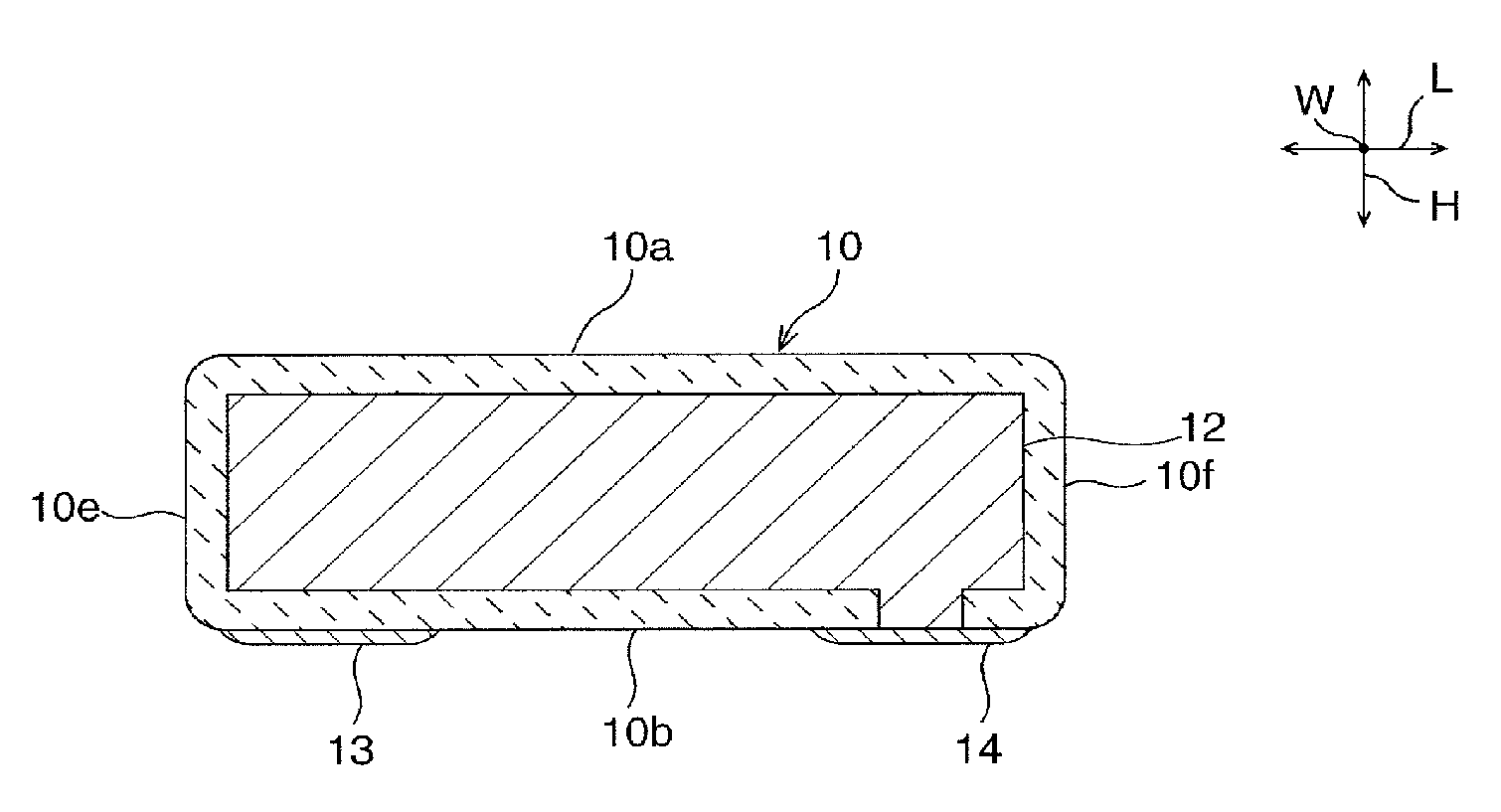
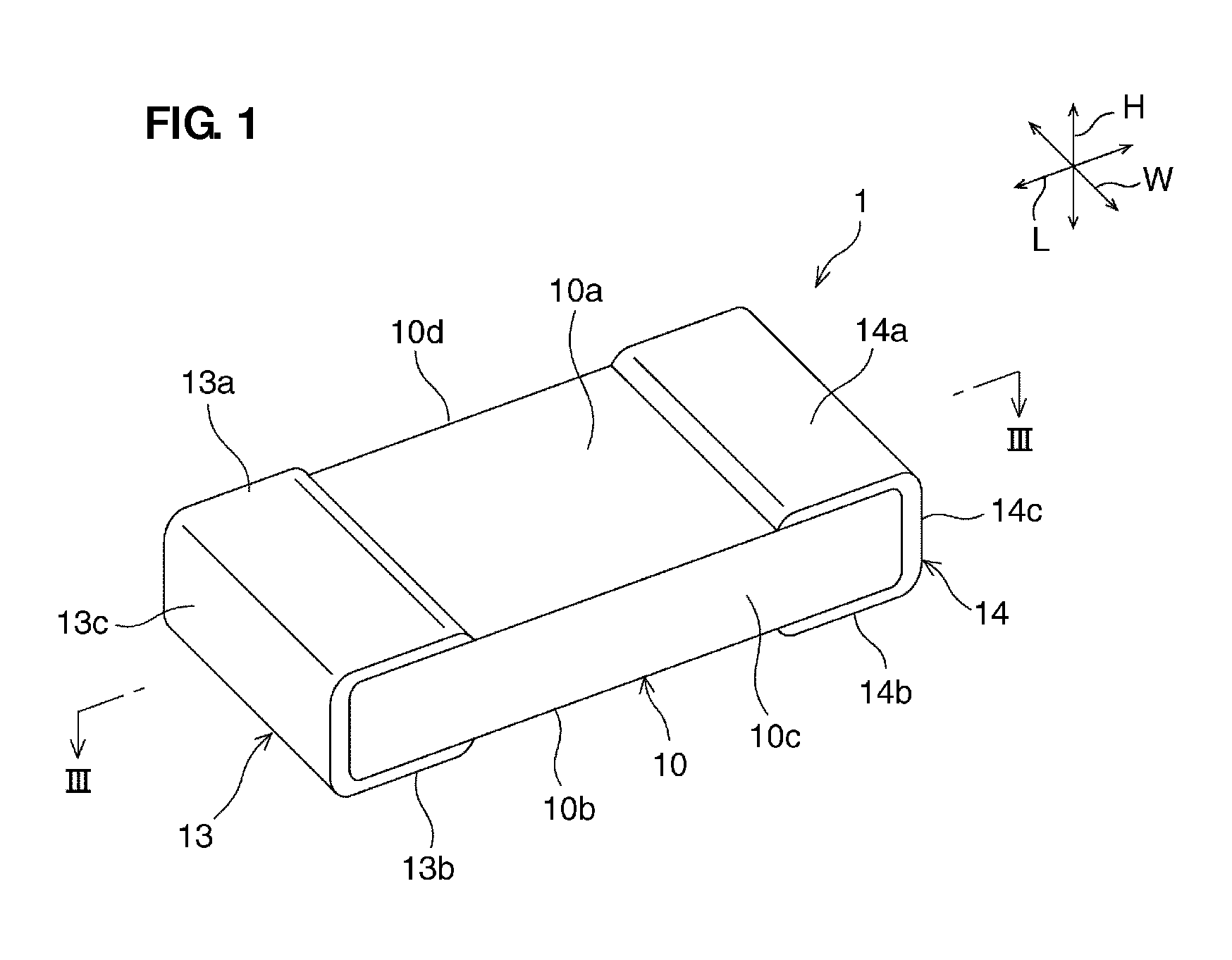
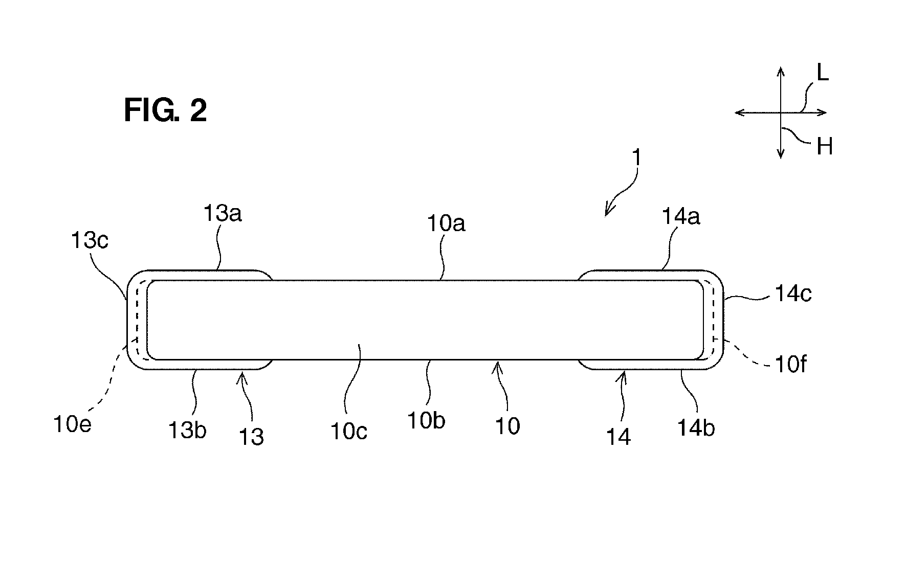
[0111]Dimension of ceramic electronic component: about 1.0 mm×about 0.5 mm×about 0.15 mm

[0112]Volume of ceramic electronic component: about 10 nF

[0113]Rated working voltage of ceramic electronic component: about 6.3 V

[0114]Primary component of ceramic material constituting ceramic element assembly: BaTiO3

[0115]Underlying electrode layer: about 50 percent by volume of Ni is included as the metal that is diffusible in Cu.

[0116]Furthermore, about 50 percent by volume of ceramic bonding material is included.

[0117]Condition of formation of underlying electrode layer: firing at about 1,200° C. for about 2 hours

[0118]Thickness of underlying electrode layer: ab...


PUM

PropertyMeasurementUnit
widthaaaaaaaaaa
widthaaaaaaaaaa
widthaaaaaaaaaa

Abstract

A ceramic electronic component includes a ceramic element assembly and external electrodes. The external electrodes are disposed on the ceramic element assembly. The external electrodes include an underlying electrode layer and a first Cu plating film. The underlying electrode layer is disposed on the ceramic element assembly. The first Cu plating film is disposed on the underlying electrode layer. The underlying electrode layer includes a metal that is diffusible in Cu and a ceramic bonding material. The metal that is diffusible in Cu is diffused in at least a surface layer in the underlying electrode layer side of the first Cu plating film.

Description

BACKGROUND OF THE INVENTION[0001]1. Field of the Invention[0002]The present invention relates to a ceramic electronic component and a method for manufacturing the same. In particular, the present invention relates to an embedded ceramic electronic component, which is arranged to be embedded in a wiring board, and a method for manufacturing the same.[0003]2. Description of the Related Art[0004]In recent years, along with miniaturization and thickness reduction of electronic apparatuses, e.g., cellular phones and portable music players, wiring boards mounted on the electronic apparatuses have been miniaturized.[0005]Japanese Unexamined Patent Application Publication No. 2002-100875 discloses a method for miniaturizing a wiring board in which a ceramic electronic component is embedded inside of a wiring board and, in addition, wiring to the ceramic electronic component is formed by using a via hole disposed on the ceramic electronic component. According to this method, it is not necess...

Claims


Application Information

Patent Timeline
Patent Type & Authority Applications(United States)
IPC IPC(8): H05K1/09B05D3/02B05D5/12
CPCH01G4/232H01G4/30H05K1/182H01F27/2804H01L41/083H01C7/008H01G4/12H10N30/50H10N30/8554H01F27/28H01G4/008
Inventor NISHISAKA, YASUHIROSANADA, YUKIOSATOMATSUMOTO, SEIICHI
Owner MURATA MFG CO LTD
Why Eureka
Try Eureka