Quantum dot light emitting diode device and display device therewith

a light-emitting diode and quantum dot technology, applied in semiconductor/solid-state device manufacturing, semiconductor devices, electrical devices, etc., can solve the problems of poor light-emitting efficiency, poor light-emitting efficiency, and limited light-emitting efficiency of organic light-emitting diodes

Active Publication Date: 2011-12-01
LG DISPLAY CO LTD +1
View PDF4 Cites 63 Cited by
  • Summary
  • Abstract
  • Description
  • Claims
  • Application Information

AI Technical Summary

Benefits of technology

[0024]An object of the present invention is to provide a quantum dot light emitting diode device in which a hole transportation layer is formed after forming a quantum dot light emitting layer by a solution process to from an inverted type quantum dot light emitting diode device for making free selection of a hole transportation layer material that enables easy injection of a hole to the quantum dot light emitting layer, a display device therewith, and methods for fabricating the same.

Problems solved by technology

Though an Organic Light Emitting Diode OLED which uses the organic light emitting material produces single color of white, red, blue or so on depending on a kind of the device, the organic light emitting diode has a limitation in expressing many color lights brilliantly.
Consequently, it can be foreseen that the hole injection into the quantum dot light emitting layer 30 is difficult to cause poor light emitting efficiency, to require a high driving voltage for making the quantum dot light emitting layer 30 to emit the light and to have poor light emitting efficiency.
First, the great hole energy barrier between the hole transport layer and the quantum dot light emitting layer makes hole transportation to the quantum dot light emitting layer difficult, to require a high driving voltage, and to cause poor light emitting efficiency due to the difficulty in transportation of the hole.

Method used


Image

  • Quantum dot light emitting diode device and display device therewith
  • Quantum dot light emitting diode device and display device therewith
  • Quantum dot light emitting diode device and display device therewith

Examples


first embodiment

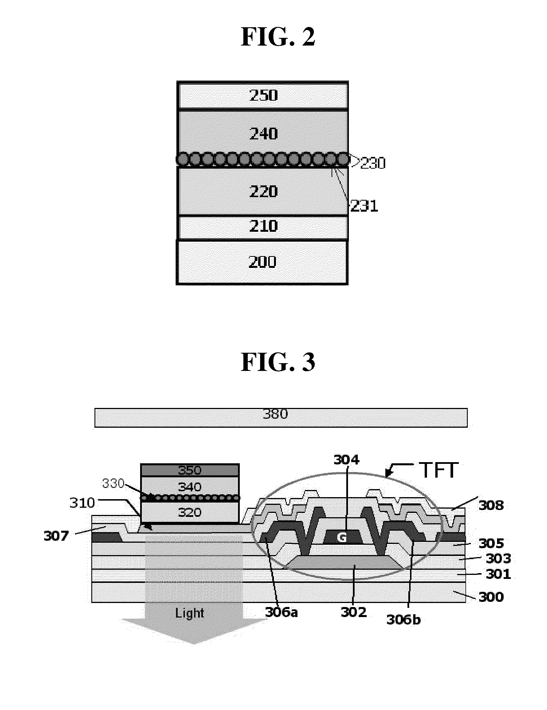
[0067]FIG. 3 illustrates a section of a display device in accordance with a first preferred embodiment of the present invention.

[0068]Referring to FIG. 3, the display device which is a bottom emission type includes a transparent cathode 310 on a substrate 300, a quantum dot light emitting layer 330 formed on the cathode 310 to have quantum dots, an anode 350 on the quantum dot light emitting layer 330, and a thin film transistor TFT connected to the cathode 310.

[0069]The display device can further include an electron transport layer 320 between the cathode 310 and the quantum dot light emitting layer 330, and a hole transport layer 340 between the quantum dot light emitting layer 330 and the anode 350.

[0070]The cathode 310 is formed of a transparent conductive metal, such as ITO, IZO, ITZO, AZO for downward light emission, and the anode 350 is formed of a non-transparent metal. For an example, the anode 350 can be formed of one selected from Calcium Ca, aluminum Al, magnesium Mg, si...

second embodiment

[0090]FIG. 4 illustrates a section of a display device in accordance with a second preferred embodiment of the present invention.

[0091]Referring to FIG. 4, the display device includes a cathode 410 on a substrate 400, a quantum dot light emitting layer 430 formed on the cathode 410 to have quantum dots, a transparent anode 450 on the quantum dot light emitting layer 430, and a thin film transistor TFT connected to the cathode 410.

[0092]The display device can further include an electron transport layer 420 between the cathode 410 and the quantum dot light emitting layer 430, and a hole transport layer 440 between the quantum dot light emitting layer 430 and the anode 450.

[0093]The anode 450 is formed of a transparent conductive metal, such as ITO, IZO, ITZO, AZO for upward light emission, and the cathode 410 is formed of a non-transparent metal. For an example, the anode 450 can be formed of one selected from Calcium Ca, aluminum Al, magnesium Mg, silver Ag, barium Ba, or an alloy in...

third embodiment

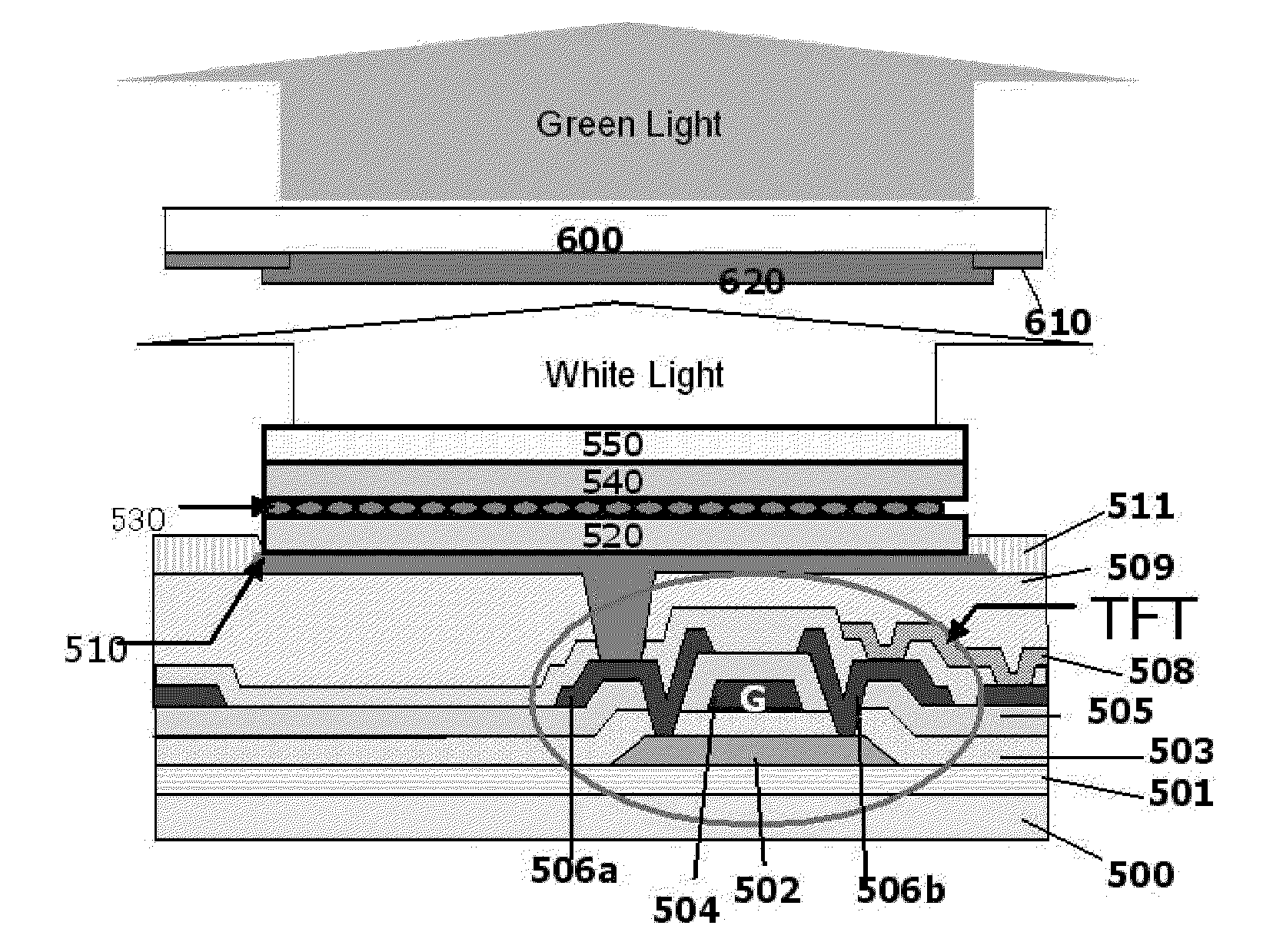
[0098]FIG. 5 illustrates a section of a display device in accordance with a third preferred embodiment of the present invention.

[0099]Referring to FIG. 5, the display device includes a cathode 510 on a first substrate 500, a quantum dot light emitting layer 530 formed on the cathode 510 to have quantum dots 531, a transparent anode 550 on the quantum dot light emitting layer 530, a thin film transistor TFT formed on the first substrate 500 connected to the cathode 510, and a second substrate 600 formed opposite to the first substrate 500 to have a color filter layer 620.

[0100]The display device can further include an electron transport layer 520 between the cathode 510 and the quantum dot light emitting layer 530, and a hole transport layer 540 between the quantum dot light emitting layer 530 and the anode 550.

[0101]The quantum dot light emitting diode device QLED on the first substrate 500 and the TFT are identical to a structure on the substrate in the second embodiment.

[0102]Howe...


PUM


Abstract

The present invention relates to a quantum dot light emitting diode device in which a hole transportation layer is formed after forming a quantum dot light emitting layer by a solution process by applying an inverted type quantum dot light emitting diode device for making free selection of a hole transportation layer material that enables easy injection of a hole to the quantum dot light emitting layer; and display device and method therewith.

Description

CROSS REFERENCE TO RELATED APPLICATION[0001]This application claims the benefit of the Patent Korean Application No. 10-2010-0048569, filed on May 25, 2010, which is hereby incorporated by reference as if fully set forth herein.BACKGROUND OF THE DISCLOSURE[0002]1. Field of the Disclosure[0003]The present invention relates to quantum dot light emitting diode devices, and more particularly to a quantum dot light emitting diode device in which a hole transport layer is formed after forming a quantum dot light emitting layer by a solution process to form an inverted type quantum dot light emitting diode device for making free selection of a hole transport layer material that enables easy injection of a hole to the quantum dot light emitting layer; and a display device therewith.[0004]2. Discussion of the Related Art[0005]Importance of the display device is being further emphasized as a visual information transmission media in an information oriented society, and in order to occupy a maj...

Claims


Application Information

Patent Timeline
Patent Type & Authority Applications(United States)
IPC IPC(8): H01L33/06H01L33/42H01L33/08
CPCH01L27/3244H01L51/5036H01L51/502H01L51/5004H10K59/00H10K50/115H10K71/00H10K59/12H10K50/11H10K2101/40H10K50/125
Inventor KIM, YOUNG-MIKANG, HO-CHEOLKIM, HO-JINLEE, CHANG-HEECHAR, KOOK-HEONLEE, SEONG-HOONKWAK, JEONG-HUNBAE, WAN-KILEE, DONG-GULIM, JAE-HOON
Owner LG DISPLAY CO LTD
Why Eureka
Try Eureka