

Three-dimensional semiconductor memory device and method for manufacturing the same
- Summary
- Abstract
- Description
- Claims
- Application Information
AI Technical Summary
Benefits of technology
Problems solved by technology
Method used
Image

Examples
first embodiment
[0086]Hereinafter, referring to FIGS. 2 and 7 to 13, a method for manufacturing the three-dimensional semiconductor memory device according to the inventive concept will be described.
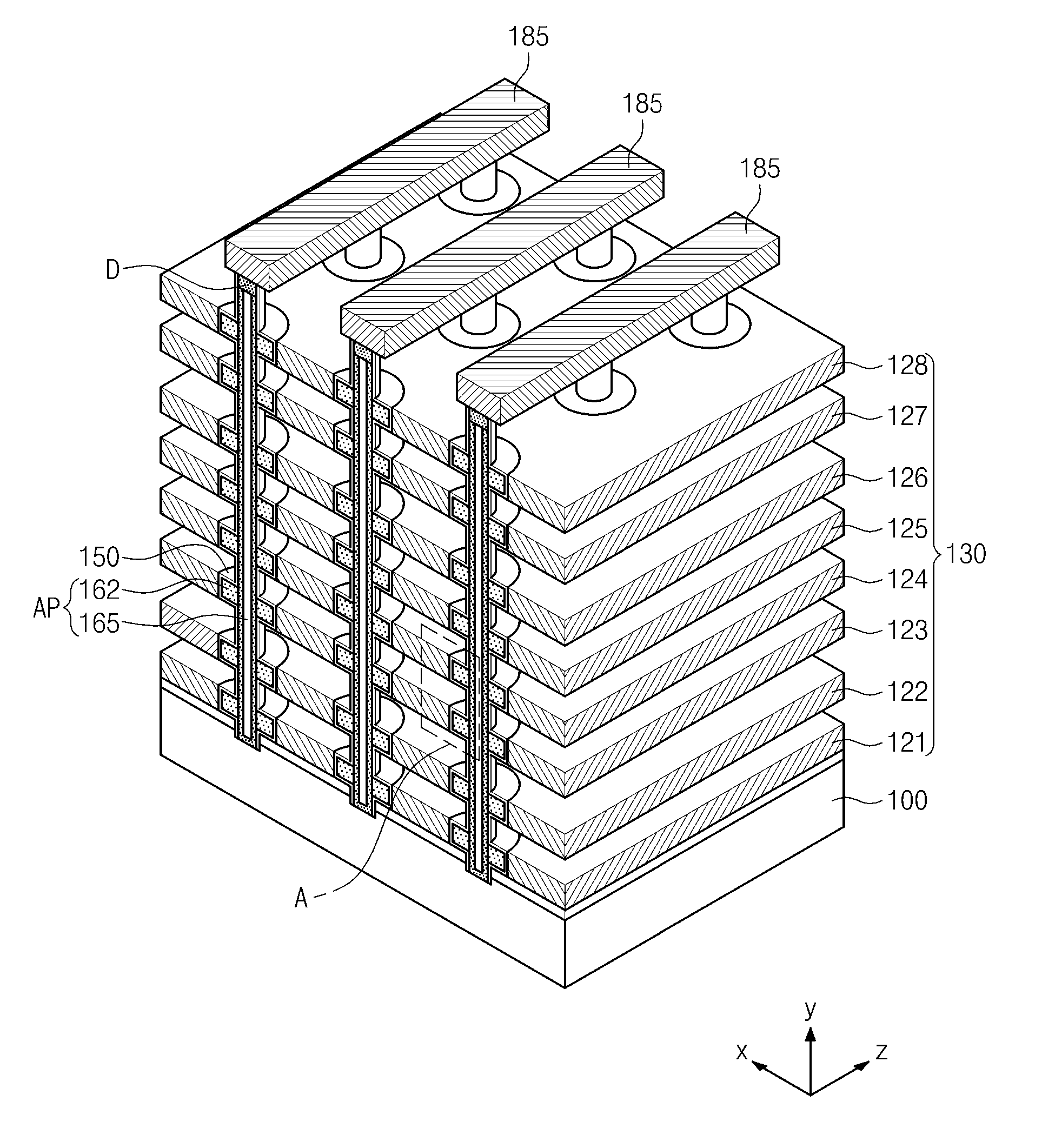
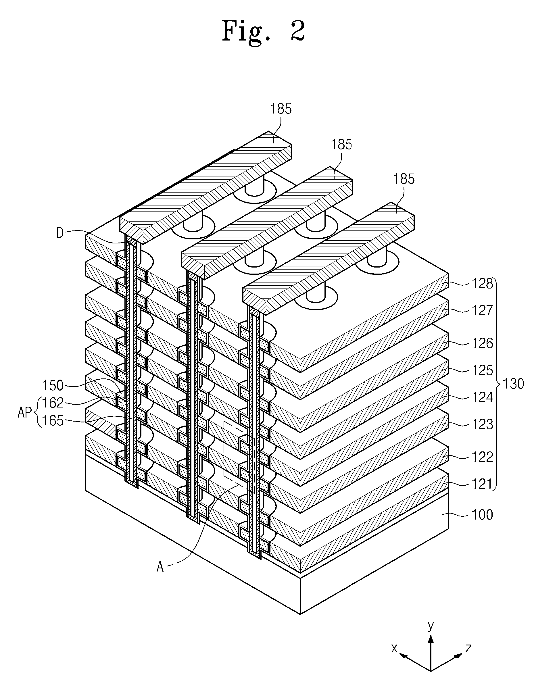
[0087]Referring to FIG. 7, the thin layer structure 130 is formed on the substrate 100. The substrate 100 may include at least one of a material having semiconductor characteristics (e.g., silicon wafer), a dielectric material (e.g., glass), or semiconductor or conductor covered with a dielectric material.
[0088]The thin layer structure 130 may include the plurality of interlayer dielectrics 111 to 119 and the plurality of gate conductive layers 121 to 128. The interlayer dielectrics 111 to 119 and the gate conductive layers 121 to 128 may be alternately stacked on the substrate. For instance, the interlayer dielectrics 111 to 119 may be at least one of thermal oxide layer, silicon oxide layer, silicon nitride layer, and silicon oxynitride layer. The gate conductive layers 121 to 128 may be formed of at ...
second embodiment
[0147]Hereinafter, referring to FIGS. 25 to 35, a method for manufacturing the three-dimensional semiconductor memory device according to the inventive concept will be described.
[0148]Referring to FIG. 25, a thin layer structure 230 may be formed on the substrate 200. The substrate 200 may include a material having semiconductor characteristics (e.g., silicon wafer), a dielectric material (e.g., glass), and / or a semiconductor or conductor covered with a dielectric material.
[0149]The thin layer structure 230 may include a plurality of interlayer dielectrics 211 to 219 and a plurality of sacrificial layers 221 to 228. As illustrated in FIG. 25, the interlayer dielectrics 211 to 219 and the sacrificial layers 221 to 228 may be alternately and repeatedly stacked. The interlayer dielectrics 211 to 219 and the sacrificial layers 221 to 228 may be formed of materials selected to have an etch selectivity. For instance, the interlayer dielectrics 211 to 219 may be at least one of silicon oxi...
PUM
 Abstract
Description
Claims
Application Information