Semiconductor device

a technology of semiconductor devices and diodes, applied in semiconductor devices, semiconductor/solid-state device details, electrical apparatus, etc., can solve the problem of more likely to be affected and achieve the effect of improving the accuracy with which the diode electric current is detected, good accuracy, and reducing the space taken up by the electric current detection region

Active Publication Date: 2011-12-08
DENSO CORP
View PDF6 Cites 19 Cited by
  • Summary
  • Abstract
  • Description
  • Claims
  • Application Information

AI Technical Summary

Benefits of technology

[0016]According to the construction noted above, in addition to the IGBT electric current, the diode electric current can also be detected with good accuracy by utilizing the first electric current detection region. Compared to when two electric current detection regions are used to detect the IGBT electric current and the diode electric current, the space taken up by the electric current detection regions can be reduced.
[0017]The technique disclosed herein is also effective when only the diode electric current detection region capable of detecting the diode electric current is formed in the semiconductor

Problems solved by technology

However, because the electric current detection region is significantly small compared to the main active region, the electric current detection region is m

Method used


Image

  • Semiconductor device
  • Semiconductor device
  • Semiconductor device

Examples


embodiment 1

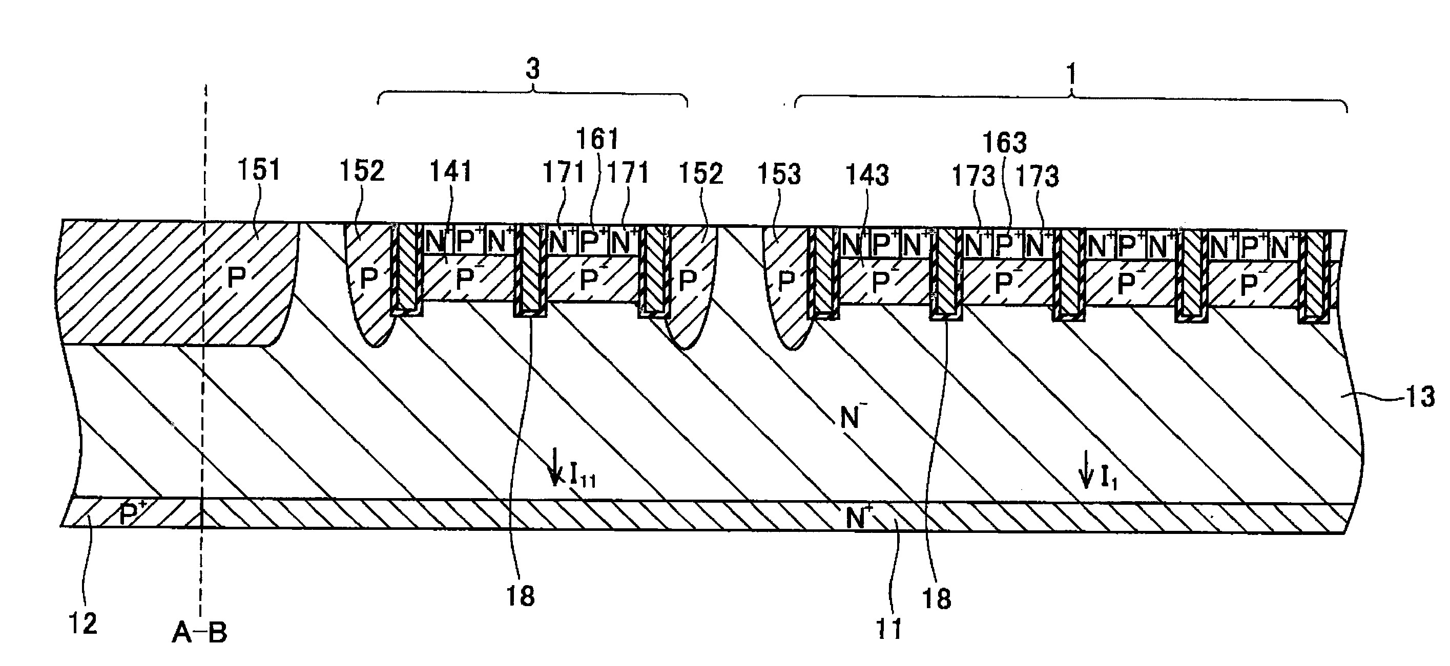
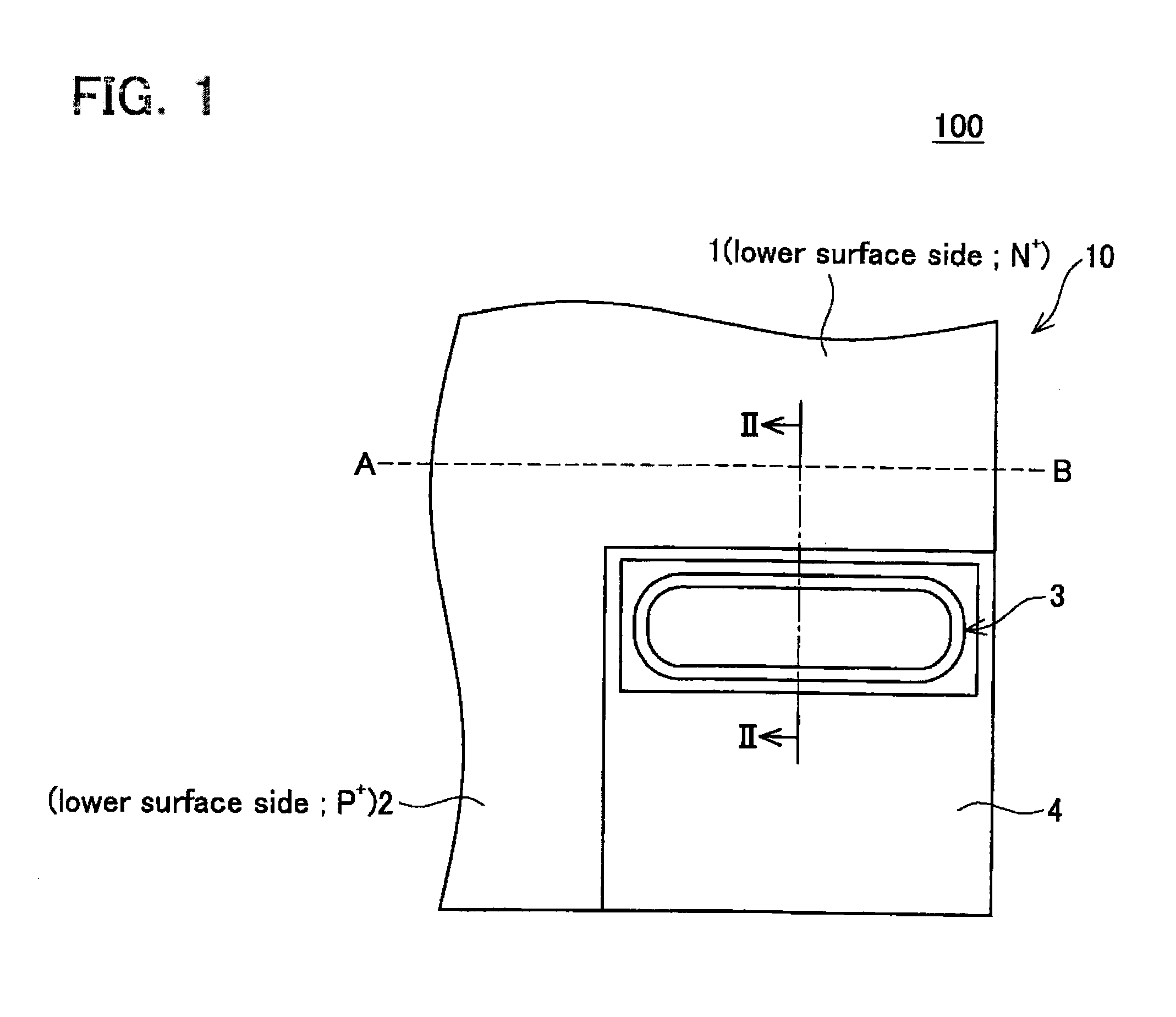
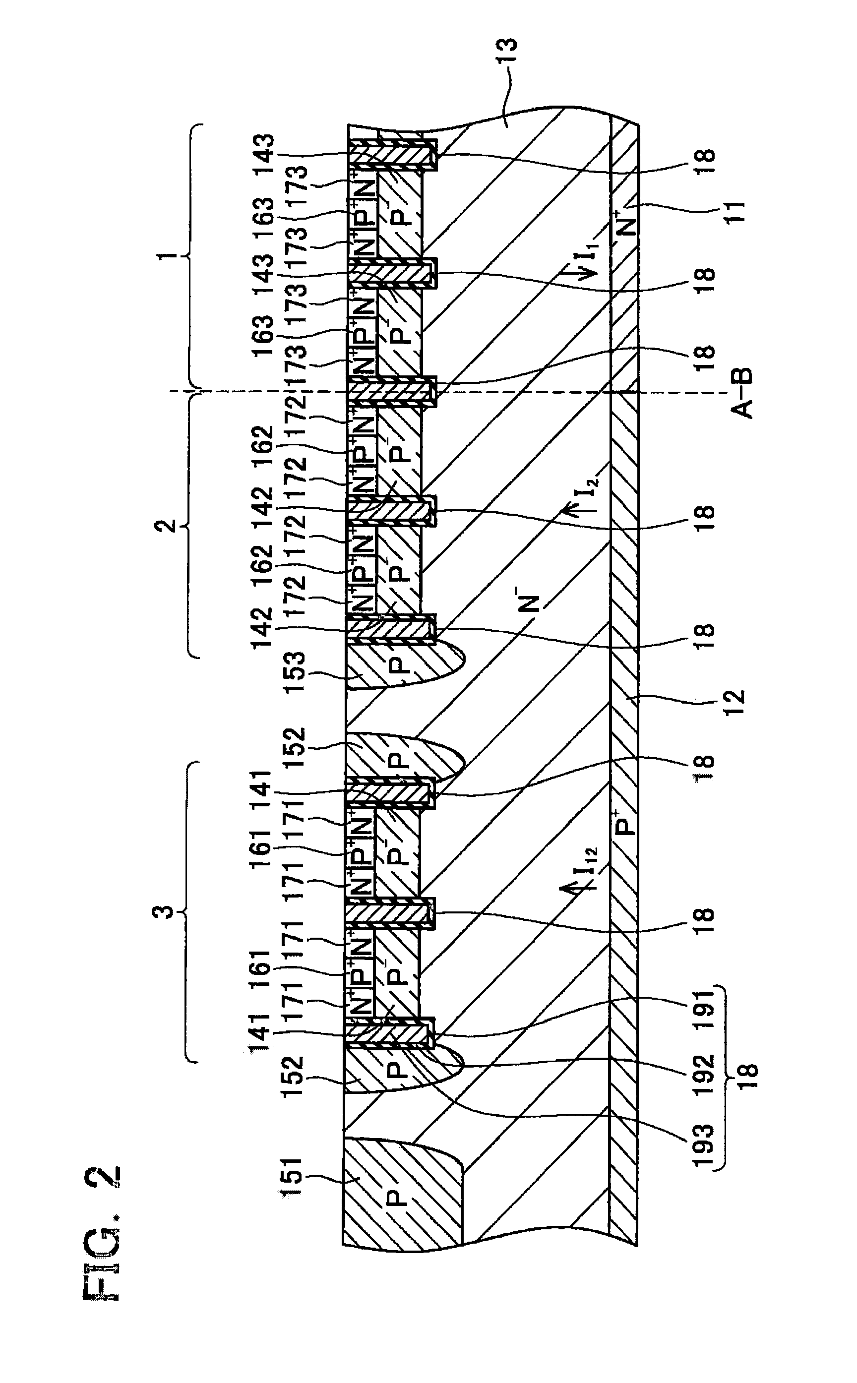
[0028]Embodiment 1 of the present teachings will be explained with reference to the drawings. FIG. 1 is a schematic plan view of a semiconductor device 100, and shows the area around a boundary portion between a main active region and an electric current detection region. FIG. 2 is a schematic expanded cross-sectional view along line II-II of FIG. 1.

[0029]As shown in FIGS. 1 and 2, the semiconductor device 100 comprises a diode main region 1, an IGBT main region 2, an electric current detection region 3, and a diffusion layer region 4 that are formed in a semiconductor substrate 10. The semiconductor substrate 10 comprises a first N+ layer 11; a first P+ layer 12 adjacent to the first N+ layer 11; an N− layer 13 formed on the surfaces of the first N+ layer 11 and the first P+ layer 12; and N− layers 141, 142, 143 and P layers 151, 152, 153 formed on the surface of the N− layer 13. Second P+ layers 161, 162, 163 and second N+ layers 171, 172, 173 are respectively arranged on the surf...

embodiment 2

[0043]FIG. 3 is a schematic plan view of a semiconductor device 200 according to the present embodiment, and shows the area around a boundary portion between a main active region and an electric current detection region on a semiconductor substrate. FIG. 4 is a schematic expanded cross-sectional view along line IV-IV of FIG. 3.

[0044]With the semiconductor device 200, the position of the boundary (broken line AB) between the first P+ layer 12 and the first N+ layer 11 formed in the lower surface side of the semiconductor substrate 20 differs from that of the semiconductor device 100. In the main active region, the region comprising the first N+ layer 11 and the layers formed on the surface thereof becomes the diode main region 1, and the region comprising the first P+ layer 12 and the layers formed on the surface thereof becomes the IGBT active region 2. Like with the diode main region 1, the electric current detection region 3 is arranged in the first N+ layer 11 on the upper surfac...

embodiment 3

[0055]FIG. 5 is a schematic plan view of a semiconductor device 300 according to the present embodiment, and shows the area around a boundary portion between a main active region and an electric current detection region on a semiconductor substrate. FIG. 6 is a schematic expanded cross-sectional view along line VI-VI of FIG. 5.

[0056]As shown in FIGS. 5 and 6, an electric current detection region 31 and an electric current detection region 32 are located on the semiconductor device 300. In addition, the boundary (broken line AB) between the first P+ layer 12 and the first N+ layer 11 formed in the lower surface side of the semiconductor substrate 30 is positioned on an inactive region between the electric current detection region 31 and the electric current detection region 32. The electric current detection region 31 and the electric current detection region 32 are respectively surrounded by the P layer 152 like with the electric current detection region 3 of Embodiment 1. Because t...


PUM


Abstract

A reverse conducting semiconductor device having an IGBT element region and a diode element region in one semiconductor substrate is provided. An electric current detection region is arranged adjacent to the IGBT element region, and a collector region of the IGBT element region is extended to connect with a collector region of the electric current detection region. Instability in the IGBT detection current caused by a boundary portion between the IGBT and the diode can be suppressed. In the same way, an electric current detection region is arranged adjacent to the diode element region, and a cathode region of the diode element region is extended to connect with a cathode region of the electric current detection region. Instability in the diode detection current caused by the boundary portion between the IGBT and the diode can be suppressed.

Description

TECHNICAL FIELD[0001]The present invention relates to a semiconductor device in which both an insulated gate bipolar transistor (IGBT) element region and a diode element region are formed in one semiconductor substrate.BACKGROUND ART[0002]For the purpose of protecting against damage due to an overimposed current, etc., a semiconductor device is provided with an electric current detection region to detect electric current flowing through the semiconductor device. Japanese Patent Application Publication No. H7-245394 discloses a semiconductor device having a main active region (main cell region) in which an IGBT is formed, and an electric current detection region (detector cell region) for detecting electric current that flows through the main active region provided in one semiconductor substrate. An IGBT identical to that on the main active region is formed in the electric current detection region, and the electric current detection region is spaced apart from the main active region ...

Claims


Application Information

Patent Timeline
IPC IPC(8): H01L27/06
CPCH01L29/0619H01L29/7397H01L29/0834H01L29/0696
Inventor SOENO, AKITAKA
Owner DENSO CORP
Why Eureka
Try Eureka