Semiconductor device
- Summary
- Abstract
- Description
- Claims
- Application Information
AI Technical Summary
Benefits of technology
Problems solved by technology
Method used
Image

Examples
embodiment 1
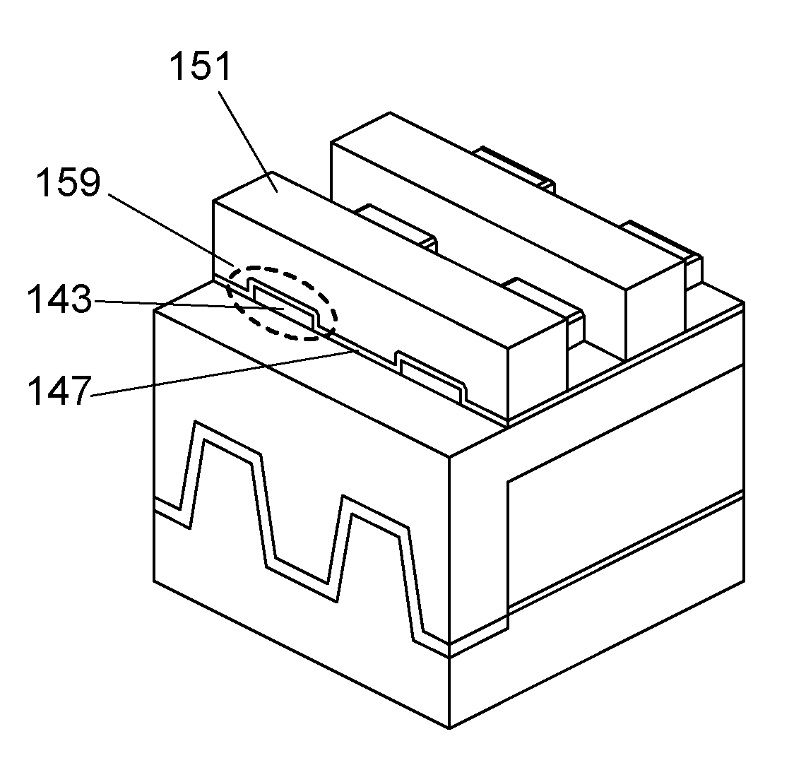
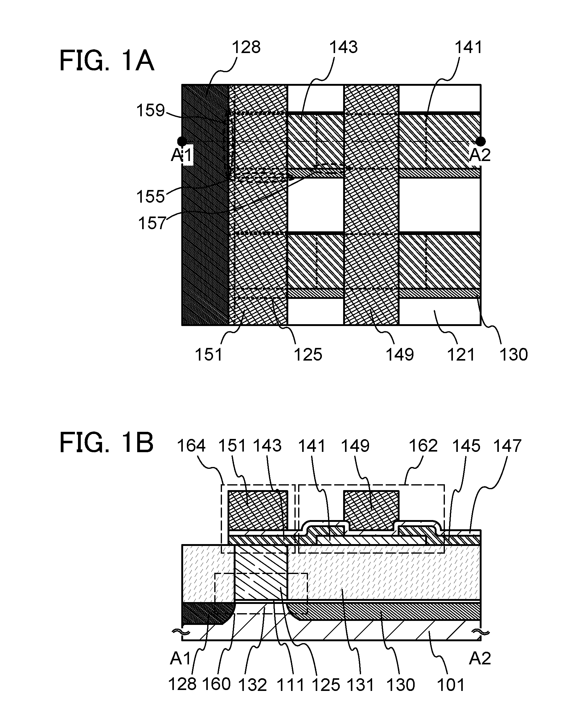
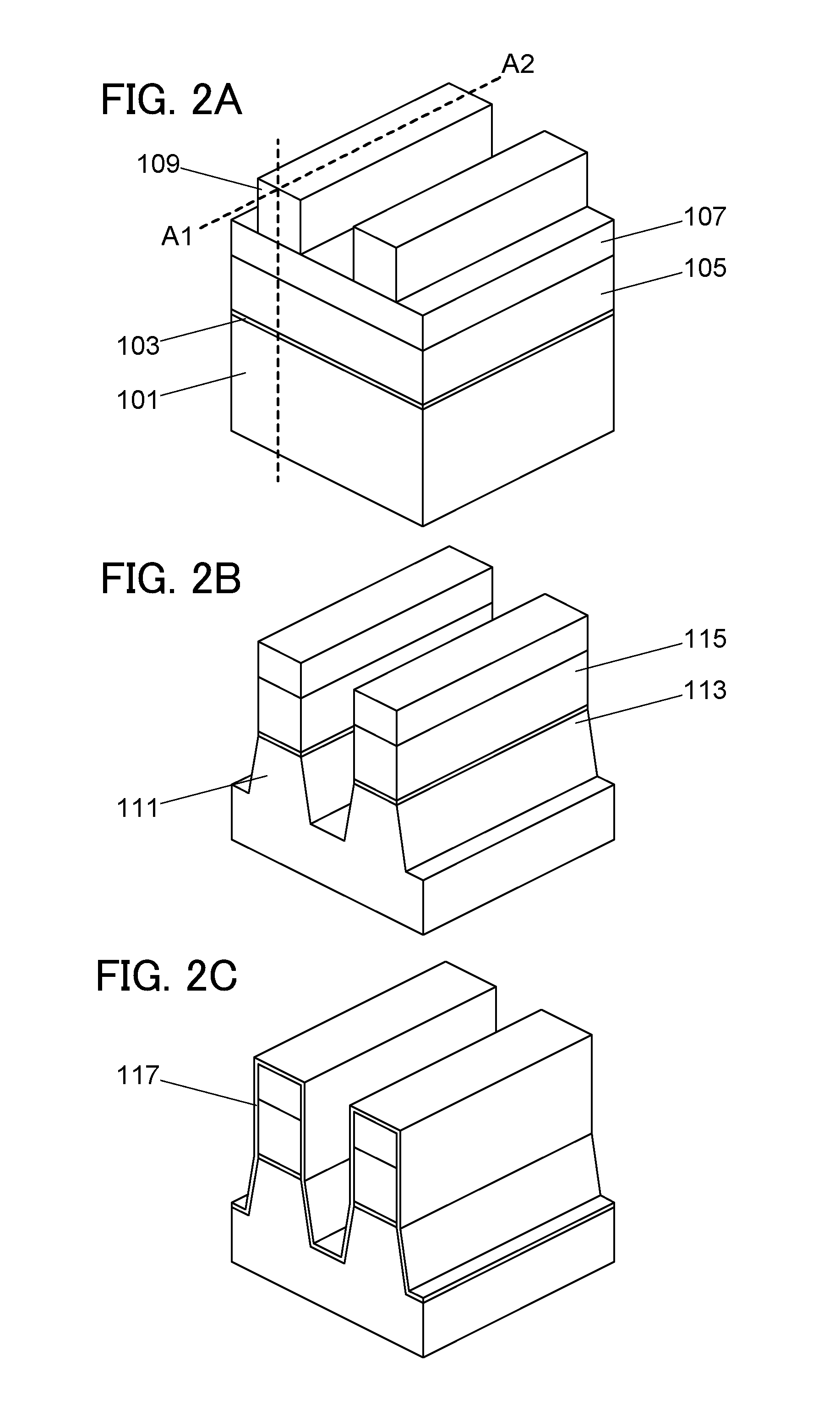
[0045]In this embodiment, a structure and a manufacturing method of a semiconductor device according to one embodiment of the disclosed invention will be described with reference to FIGS. 1A and 1B, FIGS. 2A to 2C, FIGS. 3A to 3C, FIGS. 4A to 4C, FIGS. 5A to 5C, FIGS. 6A to 6C, and FIG. 7. Note that FIGS. 1A and 1B, FIGS. 2A to 2C, FIGS. 3A to 3C, FIGS. 4A to 4C, FIGS. 5A to 5C, FIGS. 6A to 6C, and FIG. 7 illustrate part of the semiconductor device for explanation of the semiconductor device and the manufacturing method thereof and do not illustrate the entire structure of the semiconductor device.
[0046]FIGS. 1A and 1B illustrate an example of a structure of the semiconductor device. FIG. 1A is a plan view illustrating part of the semiconductor device, and FIG. 1B is a cross-sectional view taken along line A1-A2 of FIG. 1A. The semiconductor device illustrated in FIGS. 1A and 1B includes a transistor 160 including a first semiconductor material in a lower portion, and a transistor 1...
embodiment 2
[0135]In this embodiment, an example of application of a semiconductor device according to one embodiment of the disclosed invention will be described with reference to FIGS. 8A-1, 8A-2, and 8B and FIGS. 9 to 12. Here, an example of a memory device is described. Note that in some circuit diagrams, “OS” is written beside a transistor in order to indicate that the transistor includes an oxide semiconductor.
[0136]First, a basic circuit configuration and an operation thereof will be described with reference to FIGS. 8A-1, 8A-2, and 8B. In a semiconductor device illustrated in FIG. 8A-1, a first wiring (1st Line) is electrically connected to a source electrode (or a drain electrode) of a transistor 160. A second wiring (2nd Line) is electrically connected to a drain electrode (or a source electrode) of the transistor 160. A third wiring (3rd Line) is electrically connected to a source electrode (or a drain electrode) of a transistor 162. A fourth wiring (4th Line) is electrically connect...
application example
[0162]Next, a more specific circuit configuration to which the circuit illustrated in FIGS. 8A-1, 8A-2, and 8B is applied and an operation thereof will be described with reference to FIGS. 9 to 12.
[0163]FIG. 9 illustrates an example of a circuit diagram of a semiconductor device having a storage capacity of (m×n) bits.
[0164]The semiconductor device according to one embodiment of the present invention includes m (m is an integer of 2 or more) signal lines S, m word lines WL, n (n is an integer of 2 or more) bit lines BL, k (k is a natural number smaller than n) source lines SL, a memory cell array having memory cells 1100 arranged in a matrix of m rows (in the vertical direction)×n columns (in the horizontal direction), and peripheral circuits such as a first driver circuit 1111, a second driver circuit 1112, a third driver circuit 1113, and a fourth driver circuit 1114. Here, the structure illustrated in FIG. 8A-1 is applied to the memory cells 1100. The memory cells 1100 are connec...
PUM
 Abstract
Description
Claims
Application Information
 - Generate Ideas
- Intellectual Property
- Life Sciences
- Materials
- Tech Scout
- Unparalleled Data Quality
- Higher Quality Content
- 60% Fewer Hallucinations
Browse by: Latest US Patents, China's latest patents, Technical Efficacy Thesaurus, Application Domain, Technology Topic, Popular Technical Reports.
© 2025 PatSnap. All rights reserved.Legal|Privacy policy|Modern Slavery Act Transparency Statement|Sitemap|About US| Contact US: help@patsnap.com