
Eureka
For R&D, Eureka makes reading and utilizing patents & technical documents easy.
Eureka AIR
Designed for self-driven R&D workflows. Generate viable solutions, solve complex R&D challenges, empower your innovation with AI.

Eureka Materials
Designed for material experts only. Revolutionize your material R&D, from search, analyze, to developing new materials.

TechResearch
Generate reliable direction feasibility study reports for your R&D in just a few steps.

TechSeek
Discover and master advanced knowledge NOW. Basics, ideas, possibilities, all at once.

TechMind
As an expert in R&D Theories, TechMind can generates customized viable solutions instantly.

TechRisk
Analyze your overall solution with one click, know your potential R&D risks in advance.

TechMonitor
Get weekly tech updates, stay abreast of the latest tech innovations and key insights.
Pattern inspecting apparatus and pattern inspecting method
- Summary
- Abstract
- Description
- Claims
- Application Information
AI Technical Summary
Benefits of technology
Problems solved by technology
Method used
Image

Examples
embodiment 1
(1) Embodiment 1
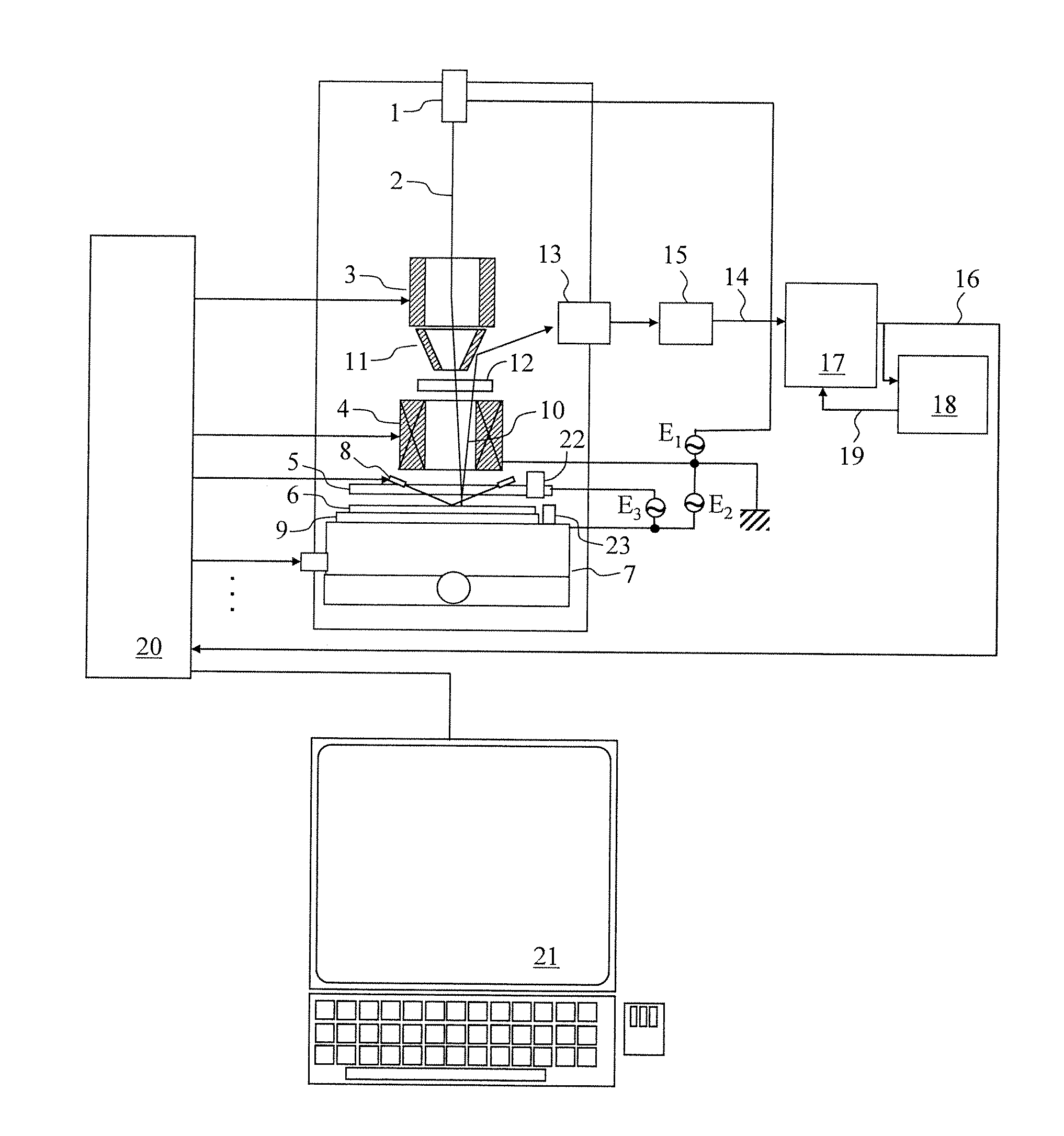
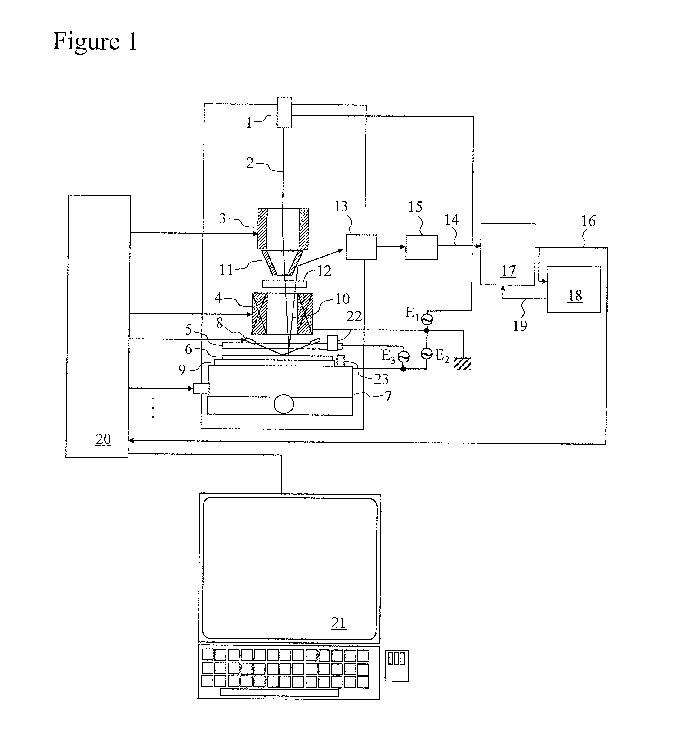
(1-1) Overall Configuration
[0030]An overall configuration example of a circuit pattern inspecting apparatus according to an embodiment is shown in FIG. 1. The circuit pattern inspecting apparatus comprises an electron source 1, a deflector 3, an objective lens 4, a charge control electrode 5, an XY stage 7, a Z sensor 8, a sample stage 9, a reflector 11, a focusing optical system 12, a sensor 13, an A / D (Analog to Digital) converter 15, a defect determination part 17, a model DB (database) part 18, an overall control part 20, a console 21, an optical microscope 22, and a standard sample piece 23.
[0031]The deflector 3 is a device that deflects electrons 2 emitted from the electron source 1. The objective lens 4 is a device that focuses the electrons 2. The charge control electrode 5 is a device that controls the electric field strength. The XY stage 7 is a device that causes a semiconductor wafer 6 including a circuit pattern to move in the XY directions. The Z sensor...
embodiment 2
(2) Embodiment 2
[0056]A modification of Embodiment 1 is described using FIG. 9. FIG. 9 illustrates a method of generating a matching result image to be displayed on the console 21 for review. In this embodiment, there is proposed a method in which the matching result image 74 and the detected image 71 are further blended. For this blending, a conversion table 81 is used. In the conversion table 81 are stored, in association with each other, degree of match attributes corresponding to the respective pixels and corresponding blending proportions α(p) (where 0≦α(p)≦1). It is noted that the p in blending proportions α(p) stands for pixel.
[0057]Thus, in the case of Embodiment 2 shown in FIG. 9, blending proportion α(p) corresponding to the degree of match of the attribute held by each pixel p of the matching result image 74 is read from the conversion table 81, and the matching result image 74 and the detected image 71 are blended pixel by pixel at blending proportions α(p) that are read...
embodiment 3
(3) Embodiment 3
[0059]A further modification of Embodiment 1 will now be described. In the case of Embodiment 1, a description was provided with respect to a case in which the detected image 71 and partial images (model images) were simply synthesized. However, by synthesizing images using the mesh warping method (a so-called morphing method) disclosed in Non-Patent Document 3, it is possible to realize a synthesized image better reflecting the information of the detected image 71. It is noted that the mesh warping technique (a so-called morphing method) applied here refers to a technique in which synthesis is performed in such a manner as to maintain the correspondence between respective feature points of the images subject to synthesis. By way of example, where there are differences in size and shape between the patterns of a partial image (model image) and the detected image 71, by synthesizing the images in such a manner as to maintain the correspondence between respective featu...
PUM
 Abstract
Description
Claims
Application Information
 - R&D Engineer
- R&D Manager
- IP Professional
- Industry Leading Data Capabilities
- Powerful AI technology
- Patent DNA Extraction
Browse by: Latest US Patents, China's latest patents, Technical Efficacy Thesaurus, Application Domain, Technology Topic, Popular Technical Reports.
© 2024 PatSnap. All rights reserved.Legal|Privacy policy|Modern Slavery Act Transparency Statement|Sitemap|About US| Contact US: help@patsnap.com