Nanowire LED structure and method for manufacturing the same

a technology of light-emitting diodes and nanowires, which is applied in the direction of nanotechnology, electrical equipment, semiconductor devices, etc., can solve the problems of difficult operation of contact material deposition using line-of-sight processes, and achieve the effects of improving lateral current spreading, reducing or eliminating discontinuities, and increasing absorption

Active Publication Date: 2011-12-22
NANOSYS INC
View PDF1 Cites 150 Cited by
  • Summary
  • Abstract
  • Description
  • Claims
  • Application Information

AI Technical Summary

Benefits of technology

[0017]In prior art methods, arrays of nanowire LEDs are contacted by depositing a contact layer that covers essentially the whole surface of the nanowires and intermediate surfaces between the nanowires using sputtering or evaporation techniques. Due to the high aspect ratio, and often small spacing of the nanowires these line-of-sight processes results in a non-conformal coverage. In particular, there is a risk that the contact layer becomes discontinuous and that the contact layer on the intermediate surfaces (e.g., the horizontal surface exposed between vertical nanowires) becomes too thin. In operation, this will result in losing the effect of some nanowires and a poor current spreading in the device, respectively. With an air-bridged p-electrode in accordance with embodiments of the invention, the risk for discontinuities is reduced or eliminated, and the lateral current spreading is improved due to a uniform thickness of the p-electrode and optional additional layers deposited on the p-electrode.
[0018]One advantage of an air-bridge p-contact or electrode for top-emitting nanowire LEDs is that a thick contact layer can directly contact the top portion of the nanowire LED. For top emitting nanowire LEDs, a transparent p-contact layer is used. Without the air-bridge, the p-electrode layer at the nanowire top portion must be made much thicker, which increases absorption.
[0019]One advantage of the air-bridge p-contact or electrode for bottom-emitting nanowire LEDs is that the reflective p-contact layer is only arranged on the top portion of the nanowires and not the whole circumferential nanowire area. A reflective layer extending down on the whole circumferential area would give significant losses due to total internal reflection.
[0020]Thus, embodiments of the invention make it possible to obtain an efficient nanowire LED with regard to internal conductivity, light generation and coupling of light out from the nanowire LED.

Problems solved by technology

Since nanowire LEDs comprise large arrays of nanowires, thereby forming a three-dimensional surface with high aspect ratio structures, deposition of contact material using line-of-sight processes is a challenging operation.

Method used


Image

  • Nanowire LED structure and method for manufacturing the same
  • Nanowire LED structure and method for manufacturing the same
  • Nanowire LED structure and method for manufacturing the same

Examples


second embodiment

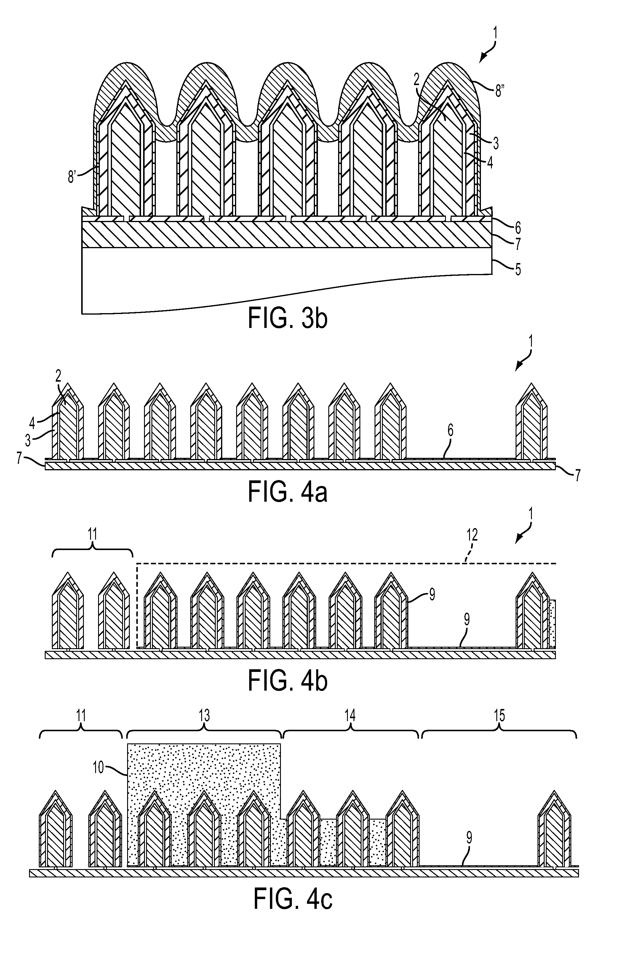
[0063]However, in an alternative second embodiment, the p-electrode is provided in a first step and the n-electrode is formed from a different material at a later stage. Such a process is discloses in FIGS. 4i to 4s and will be briefly described below. The description of the same elements and steps from FIGS. 4a-4h will not be repeated below for brevity.

[0064]The first two steps in the second embodiment method are identical to the first embodiment method, i.e. FIGS. 4a and b represent the same steps as FIGS. 4i and j. However, the protective layer 9 and masking layer 6 are not removed in the n-pad area 11FIG. 4j as in FIG. 4b.

first embodiment

[0065]In the next step, a sacrificial (e.g., resist) layer 10a is deposited in two different thicknesses such that no nanowires are left uncovered in the n-pad area 11 as in the Thus, in the left hand side of FIG. 4k it can be seen that the nanowires in area 11 are entirely covered just as the central nanowires in the non-active region 13, as opposed to in FIG. 4c where the leftmost nanowires in n-pad area 11 are completely uncovered. The nanowires in the LED area 14 are partially exposed on the top in the photoresist 10a. The p-pad area 15 is completely exposed in photoresist pattern 10a.

[0066]FIG. 4l shows that the protective layer 9 is at least partially removed from the exposed nanowire tips in LED area 13 in order to provide for contact between the p-shell 3 of the nanowires in area 13 and the p-electrode.

[0067]The p-electrode layer 16 is then deposited as shown in FIG. 4m. Layer 16 covers the entire structure. The inactive 13 and n-contact 11 areas are now covered by the pho...


PUM


Abstract

A light emitting diode (LED) structure includes a plurality of devices arranged side by side on a support layer. Each device includes a first conductivity type semiconductor nanowire core and an enclosing second conductivity type semiconductor shell for forming a pn or pin junction that in operation provides an active region for light generation. A first electrode layer extends over the plurality of devices and is in electrical contact with at least a top portion of the devices to connect to the shell. The first electrode layer is at least partly air-bridged between the devices.

Description

TECHNICAL FIELD OF THE INVENTION[0001]The present invention relates to nanowire light emitting diodes structures, in particular arrays of nanowire light emitting devices and in particular to contacting thereof.BACKGROUND OF THE INVENTION[0002]Light emitting diodes (LEDs) are increasingly used for lighting, but still there are some technological challenges to overcome, in particular with regard to large-scale processing, in order to reach the real breakthrough.[0003]Over recent years the interest in nanowire technology has increased. In comparison with LEDs produced with conventional planar technology nanowire LEDs offer unique properties due to the one-dimensional nature of the nanowires, improved flexibility in materials combinations due to less lattice matching restrictions and opportunities for processing on larger substrates. Suitable methods for growing semiconductor nanowires are known in the art and one basic process is nanowire formation on semiconductor substrates by partic...

Claims


Application Information

Patent Timeline
Patent Type & Authority Applications(United States)
IPC IPC(8): H01L33/12H01L33/60B82Y99/00
CPCB82Y20/00H01L33/08H01L33/18H01L33/38H01L33/62H01L2924/0002Y10S977/762H01L2924/00H01L33/04H01L33/20H01L33/24H01L33/42H01L33/60H01L2933/0016H01L2933/0058
Inventor LOWGREN, TRULS
Owner NANOSYS INC
Why Eureka
Try Eureka