Two-dimensional comb-drive actuator and manufacturing method thereof

a comb-drive actuator and two-dimensional technology, applied in the direction of electrostatic motors, electrostatic generators/motors, electrical apparatus, etc., can solve the problems of difficult to maintain a constant height difference between hb> and hb>, the dimension of the comb electrode structure cannot be precisely controlled, and the design of the comb-drive actuator is more complicated. , to achieve the effect of increasing the overlapping area, increasing the resultant electrostatic torque, and en

Active Publication Date: 2011-12-22
AURISE INVESTMENT CO LTD
View PDF11 Cites 6 Cited by
  • Summary
  • Abstract
  • Description
  • Claims
  • Application Information

AI Technical Summary

Benefits of technology

[0034]Specifically, the two-dimensional comb-drive actuator and manufacturing method thereof increase the overlapping area between comb electrodes, thus enlarge the rotation angle of the two-dimensional comb-drive actuator. Selectively patterned conducting layer effectively increases the resultant electrostatic torque for easily activating the rotational motion of the two-dimensional comb-drive actuator. In addition, the comb electrodes in the device layer and the conducting layer are formed using the same pattern in the present invention, so the problem of misalignment of the comb electrodes in the different layer can be solved. Furthermore, no isotropic etching is employed so the lateral undercut issue can be avoided.

Problems solved by technology

In addition, a constant biasing force may be required to activate the rotational motion of the oscillating element 104, which leads to a more complicated design for the comb-drive actuators 100.
However, during the isotropic etching step, lateral undercut will be formed in the device layer 110 such that the dimension of the comb electrode structure cannot be controlled precisely.
In addition, due to process variation, it is difficult to maintain a constant height difference between h1 and h2 on wafer batch process.

Method used


Image

  • Two-dimensional comb-drive actuator and manufacturing method thereof
  • Two-dimensional comb-drive actuator and manufacturing method thereof
  • Two-dimensional comb-drive actuator and manufacturing method thereof

Examples


first embodiment

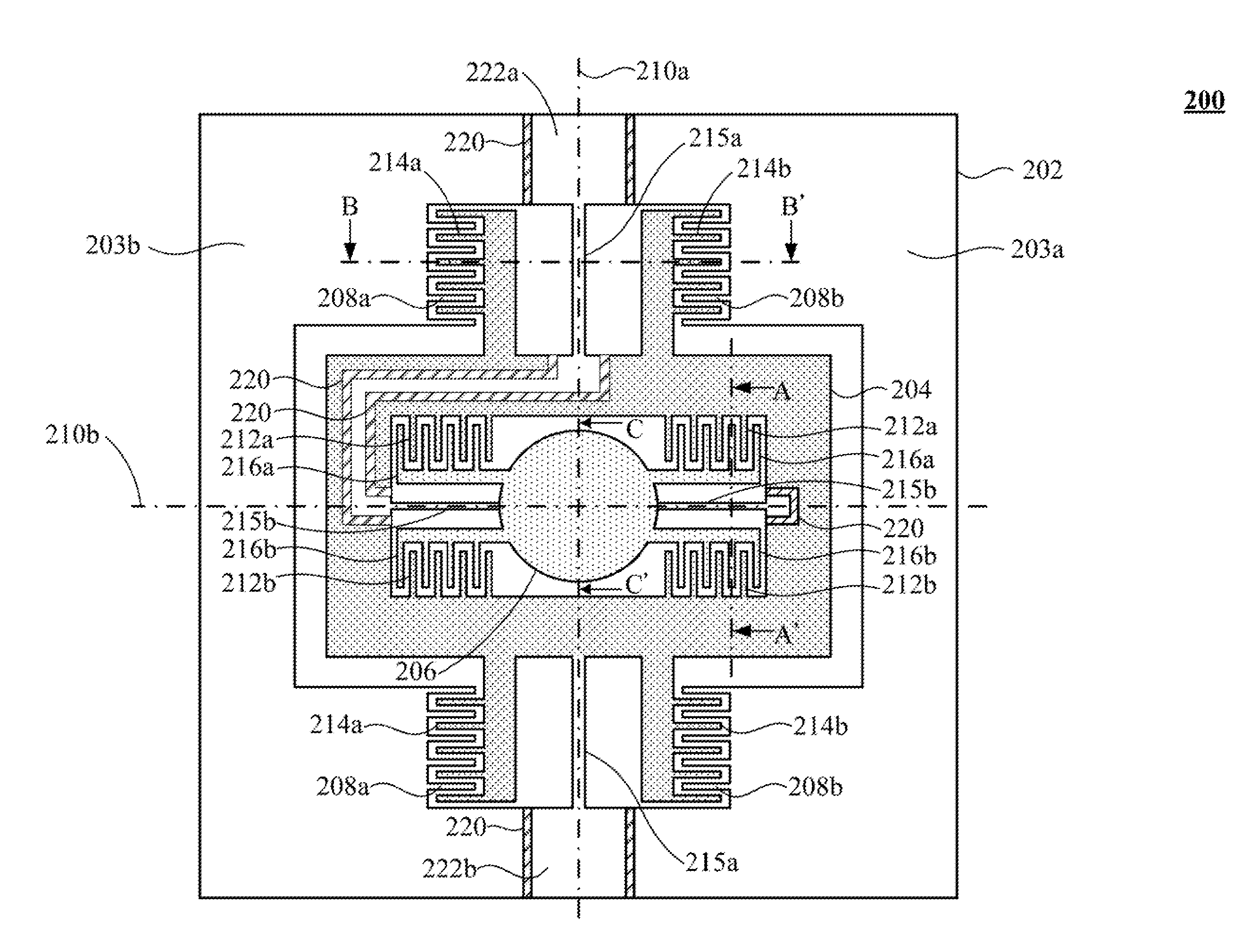
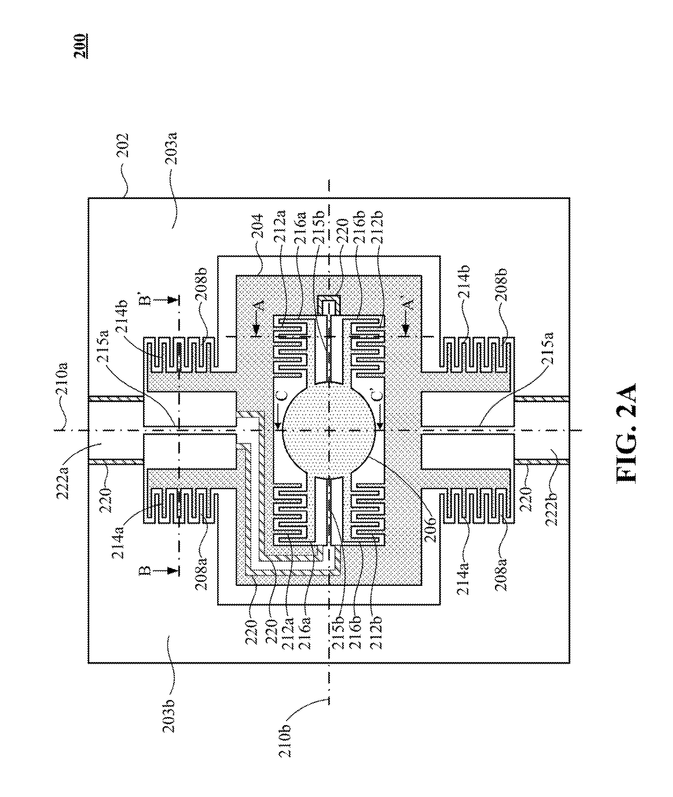
[0059]Referring to FIG. 2A and FIGS. 2B to 2E, FIGS. 2B to 2E are schematic cross-sectional views along line A-A′ of a two-dimensional comb-drive actuator 200 in FIG. 2A according to the present invention. As shown in FIGS. 2A and 2B, each of the two sets of second comb electrodes (216a, 216b) and each of the two sets of internal comb electrodes (212a, 212b) are located on the opposite sides of the second rotational axis 210b, respectively. The conducting layer 218 is selectively disposed on top of the second comb electrodes 216a and on top of the internal comb electrodes 212b, respectively such that the comb electrode thickness of combining the second comb electrodes 216a and the conducting layer 218 is greater than that of interdigitated internal comb electrodes 212a, and the comb electrode thickness of combining the internal comb electrodes 212b and the conducting layer 218 is greater than that of the interdigitated second comb electrodes 216b. The thickness of the second comb el...

second embodiment

[0071]Referring to FIG. 2A and FIGS. 4A to 4C, FIGS. 4A to 4C are schematic cross-sectional views along line A-A′ of a two-dimensional comb-drive actuator 200 in FIG. 2A according to the present invention. As shown in FIGS. 2A and 4A, each of the two sets of second comb electrodes (216a, 216b) and each of the two sets of internal comb electrodes (212a, 212b) are located on the opposite sides of the second rotational axis 210b, respectively. The conducting layer 218 is selectively disposed on top of the internal comb electrodes 212b such that the comb electrode thickness of combining the internal comb electrodes 212b and the conducting layer 218 is greater than that of the interdigitated second comb electrodes 216b. The thickness of the second comb electrodes 216a may be equal to the thickness of the interdigitated internal comb electrodes 212a.

[0072]Referring to FIG. 4A and FIG. 4B, applying a fixed electrical potential difference between the two sets of second comb electrodes (216...

third embodiment

[0074]Referring to FIG. 2A and FIGS. 5A to 5D, FIGS. 5A to 5D are schematic cross-sectional views along line B-B′ of a two-dimensional comb-drive actuator 200 shown in FIG. 2A according to the present invention. As shown in FIGS. 2A and 5A, the supporting base 202 has a substrate 202a, an insulation layer 202b and a device layer 202c which are vertically stacked. The two sets of the first comb electrodes (208a, 208b) are located on the substrate 202a and are disposed on the opposite sides of the first rotational axis 210a, respectively. The external comb electrodes (214a, 214b), disposed on device layer 202c, are interdigitated with the two sets of first comb electrodes (208a, 208b) with a vertical offset as shown in FIG. 5A. A conducting layer 218 is selectively disposed on top of the two sets of the external comb electrodes (214a, 214b) such that the comb electrode thickness of combining the conducting layer 208 and the external comb electrodes (214a, 214b) is greater than the thi...


PUM


Abstract

A two-dimensional comb-drive actuator and manufacturing method thereof are described. The two-dimensional comb-drive actuator includes a supporting base, a frame and a movable body. The supporting base has first comb electrodes and the frame has internal comb electrodes and external comb electrodes. The external comb electrodes of the frame are interdigitated to the first comb electrodes of the supporting base. The movable body has second comb electrodes which are interdigitated to the internal comb electrodes of the frame. The thicknesses of the second comb electrodes of the movable body are unequal to the internal comb electrodes of the frame and the external comb electrodes of the frame are unequal to the first comb electrodes of the supporting base. The two-dimensional comb-drive actuator utilizes a conducting layer for the above-mentioned comb electrodes in order to increase the rotation angle and operation frequency thereof.

Description

FIELD OF THE INVENTION [0001]The present invention relates to an actuator and method thereof, and more particularly to a two-dimensional comb-drive actuator and manufacturing method thereof.BACKGROUND OF THE INVENTION[0002]Recently, Micro Electro Mechanical Systems (MEMS) components featured micro structures are extensively integrated into the applications of sensing and actuating, such as accelerometers, gyroscopes, or micro scanning mirrors.[0003]FIG. 1A is a cross-sectional view of conventional comb-drive actuator 100. The comb-drive actuator 100 includes a supporting base 102 and an oscillating element 104. The supporting base 102 comprises a substrate 106, an insulation layer 108 and a device layer 110. Both the oscillating element 104 and the device layer 110 are co-planar, and the oscillating element 104 is suspended over a cavity. Due to co-planar arrangement of the comb finger electrodes, the torque generated by the comb-drive actuator 100 is insufficient to maintain the os...

Claims


Application Information

Patent Timeline
Patent Type & Authority Applications(United States)
IPC IPC(8): H02N1/00H01L21/02
CPCH02N1/006H01L21/02H02N1/008H02N1/002H02N1/00
Inventor HUNG, CHANG-LILIN, TA-WEI
Owner AURISE INVESTMENT CO LTD
Why Eureka
Try Eureka