Vertically-integrated nonvolatile memory devices having laterally-integrated ground select transistors

a nonvolatile memory and transistor technology, applied in semiconductor devices, digital storage, instruments, etc., can solve the problems of limited degree of higher integration in 2d semiconductor memory devices and high equipment requirements for reducing, and achieve the effect of low series resistan

Active Publication Date: 2011-12-22
SAMSUNG ELECTRONICS CO LTD
View PDF1 Cites 59 Cited by
  • Summary
  • Abstract
  • Description
  • Claims
  • Application Information

AI Technical Summary

Benefits of technology

According to some of these embodiments of the invention, a nonvolatile memory device includes a first common source line of first conductivity type within a semiconductor substrate. A first NAND-type string of nonvolatile memory cells is provided on the semiconductor substrate. The first NAND-type string includes a first vertically-stacked plurality of nonvolatile memory cells and a first ground select transistor electrically coupled in series with the first vertically-stacked plurality of nonvolatile memory cells. A first lateral ground select transistor is also provided, which has a source terminal within the first common source line and a drain terminal electrically connected to a source terminal of the first ground select transistor. A second NAND-type string of nonvolatile memory cells is provided at a location on the semiconductor substrate that is adjacent to the first NAND-type string. The second NAND-type string includes a second vertically-stacked plurality of nonvolatile memory cells and a second ground select transistor electrically coupled in series with the second vertically-stacked plurality of nonvolatile memory cells. A second lateral enhancement-mode ground select transistor is provided, which has a source terminal electrically connected to the drain terminal of the first lateral enhancement-mode ground select transistor and a drain terminal electrically connected to a source terminal of the second ground select transistor. To maintain a relatively low series resistance between the second NAND-type string and the first common source line, the second lateral ground select transistor is configured to have a lower threshold voltage relative to the first lateral ground select transistor.
According to additional embodiments of the invention, the first common source line includes a region of first conductivity type within a region (e.g., well region) of second conductivity type and a channel region of the first lateral ground select transistor is more heavily doped with second conductivity type dopants relative to a channel region of the second lateral ground select transistor. In some of these embodiments of the invention, a net conductivity type of the channel region of the second lateral ground select transistor is of first conductivity type. In alternative embodiments of the invention, channel region of the second lateral ground select transistor includes a region of first conductivity type and a region of second conductivity type.

Problems solved by technology

However, since high-cost equipment is required for reducing pattern size, a degree of higher integration in 2D semiconductor memory devices may become limited.

Method used


Image

  • Vertically-integrated nonvolatile memory devices having laterally-integrated ground select transistors
  • Vertically-integrated nonvolatile memory devices having laterally-integrated ground select transistors
  • Vertically-integrated nonvolatile memory devices having laterally-integrated ground select transistors

Examples


Embodiment Construction

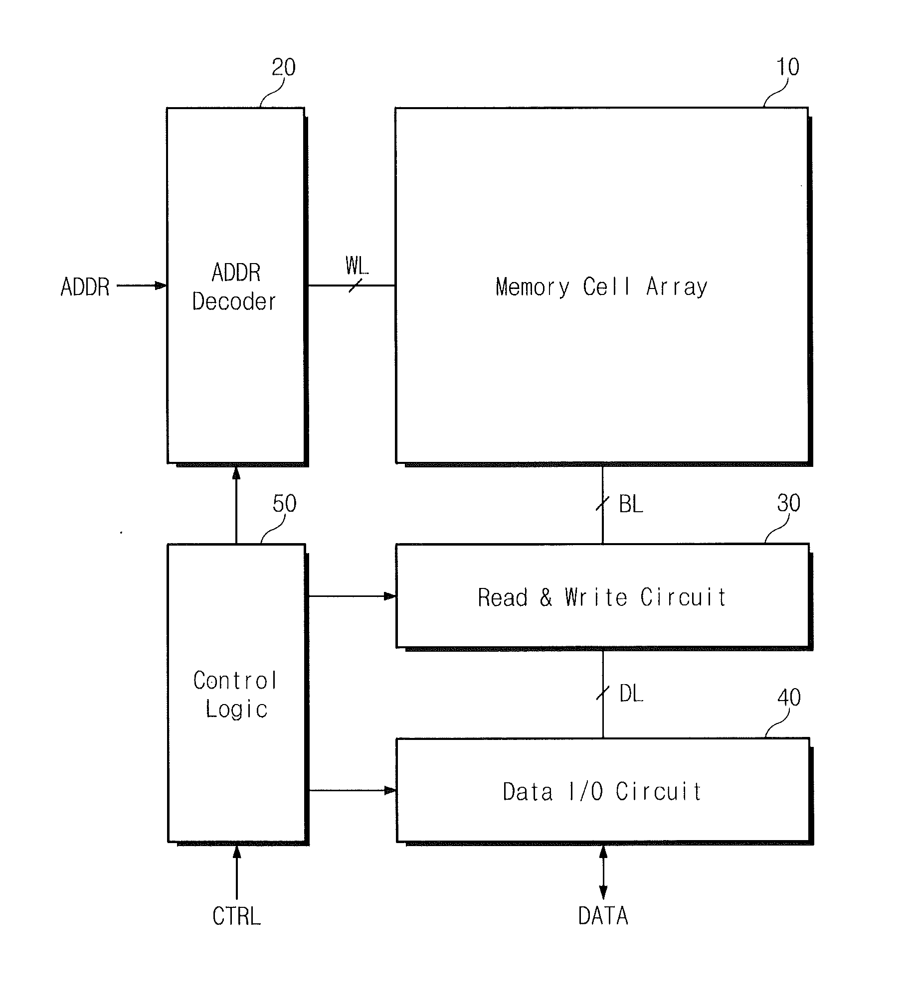
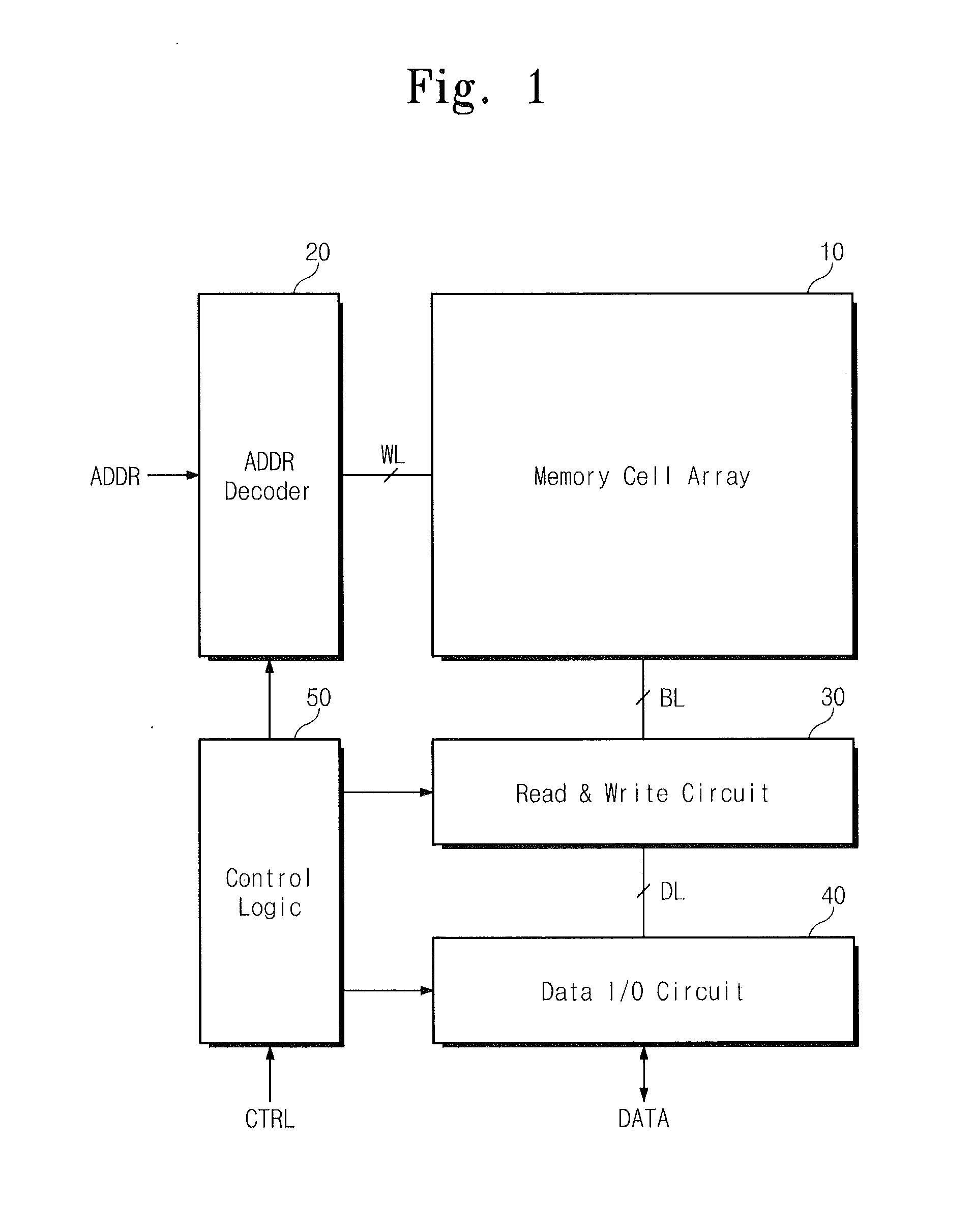
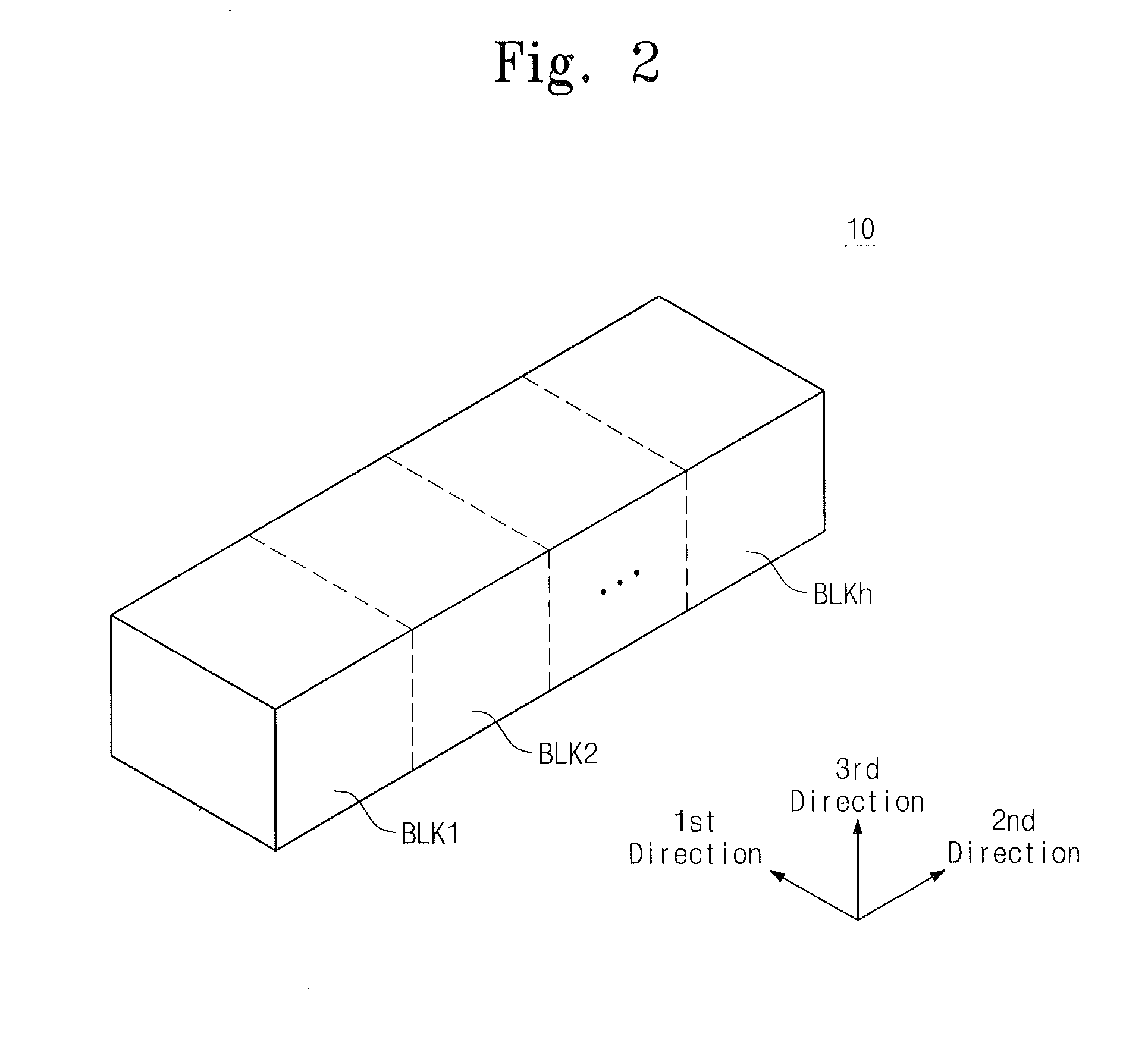
Exemplary embodiments of the inventive concept will be described below in more detail with reference to the accompanying drawings. The inventive concept may, however, be embodied in different forms and should not be construed as limited to the embodiments set forth herein. Rather, these embodiments are provided so that this disclosure will be thorough and complete, and will fully convey the scope of the inventive concept to those skilled in the art.

In embodiments of the inventive concept, an impurity-doped region may have a first conductive type or a second conductive type by doping a first conductive impurity ion and a second conductive impurity ion at different concentrations. The doping concentration of the impurity-doped region denotes a final conductive concentration with different conductive types offset.

In the specification, it will be understood that when an element such as a layer, film, region, or substrate is referred to as being “on” another element, it can be directly o...


PUM


Abstract

Nonvolatile memory devices utilize vertically-stacked strings of nonvolatile memory cells (e.g., NAND-type strings) that can be selectively coupled to common source lines within a substrate. This selective coupling may be provided by lateral ground select transistors having different threshold voltages that account for different lateral spacings between the vertically-stacked strings of nonvolatile memory cells and the common source lines.

Description

FIELD OF THE INVENTIONThe present disclosure herein relates to semiconductor devices and methods of forming same.BACKGROUND OF THE INVENTIONTo satisfy excellent performance and low cost, it is required to increase a degree of integration in semiconductor devices. Particularly, a degree of integration in memory devices is an important factor for determining the prices of products. In typical Two-Dimensional (2D) memory devices, a degree of integration is mainly determined in proportion to the occupied area of memory cells, which is affected by the level of fine pattern forming technology. However, since high-cost equipment is required for reducing pattern size, a degree of higher integration in 2D semiconductor memory devices may become limited.To overcome these limitations, Three-Dimensional (3D) memory devices including three-dimensionally arranged memory cells are being proposed. For mass production of the 3-D memory devices, however, a process technology which reduces manufacturi...

Claims


Application Information

Patent Timeline
Patent Type & Authority Applications(United States)
IPC IPC(8): G11C16/04
CPCG11C16/0408G11C16/0466G11C16/0483H01L27/11551H01L27/11556H01L27/11519H10B41/10H10B41/20H10B41/27H10B43/27H10B43/35
Inventor SHIM, SUNILJEONG, JAEHUNJANG, JAEHOONKIM, KIHYUN
Owner SAMSUNG ELECTRONICS CO LTD
Why Eureka
Try Eureka