Multiple-input comparator and power converter

a power converter and multi-input technology, applied in the field of circuit design, can solve the problems of error amplifier not functioning normally circuit is very complicated and restricted, etc., and achieves the effect of simplifying the circuit structur

Active Publication Date: 2011-12-29
WUXI ZGMICRO ELECTRONICS CO LTD
View PDF10 Cites 15 Cited by
  • Summary
  • Abstract
  • Description
  • Claims
  • Application Information

AI Technical Summary

Benefits of technology

[0017]Comparing to the prior arts, with the implementation of a current input the present invention not only is capable of performing complicated comparison functions, but also has much simpler circuit structure. Other objects, features, and advantages of the present invention will become apparent upon examining the following detailed description of an embodiment thereof, taken in conjunction with the attached drawings.

Problems solved by technology

As a result, the error amplifier does not function normally.
However, the circuit is very complicated and is restricted by the responsive speed of the operational amplifier OP1.
The circuit is very complicated and is restricted by the responsive speed of the operational amplifier OP2.

Method used


Image

  • Multiple-input comparator and power converter
  • Multiple-input comparator and power converter
  • Multiple-input comparator and power converter

Examples


first embodiment

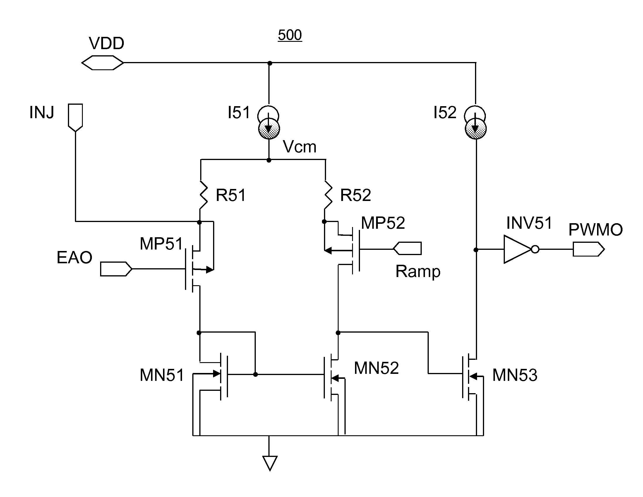
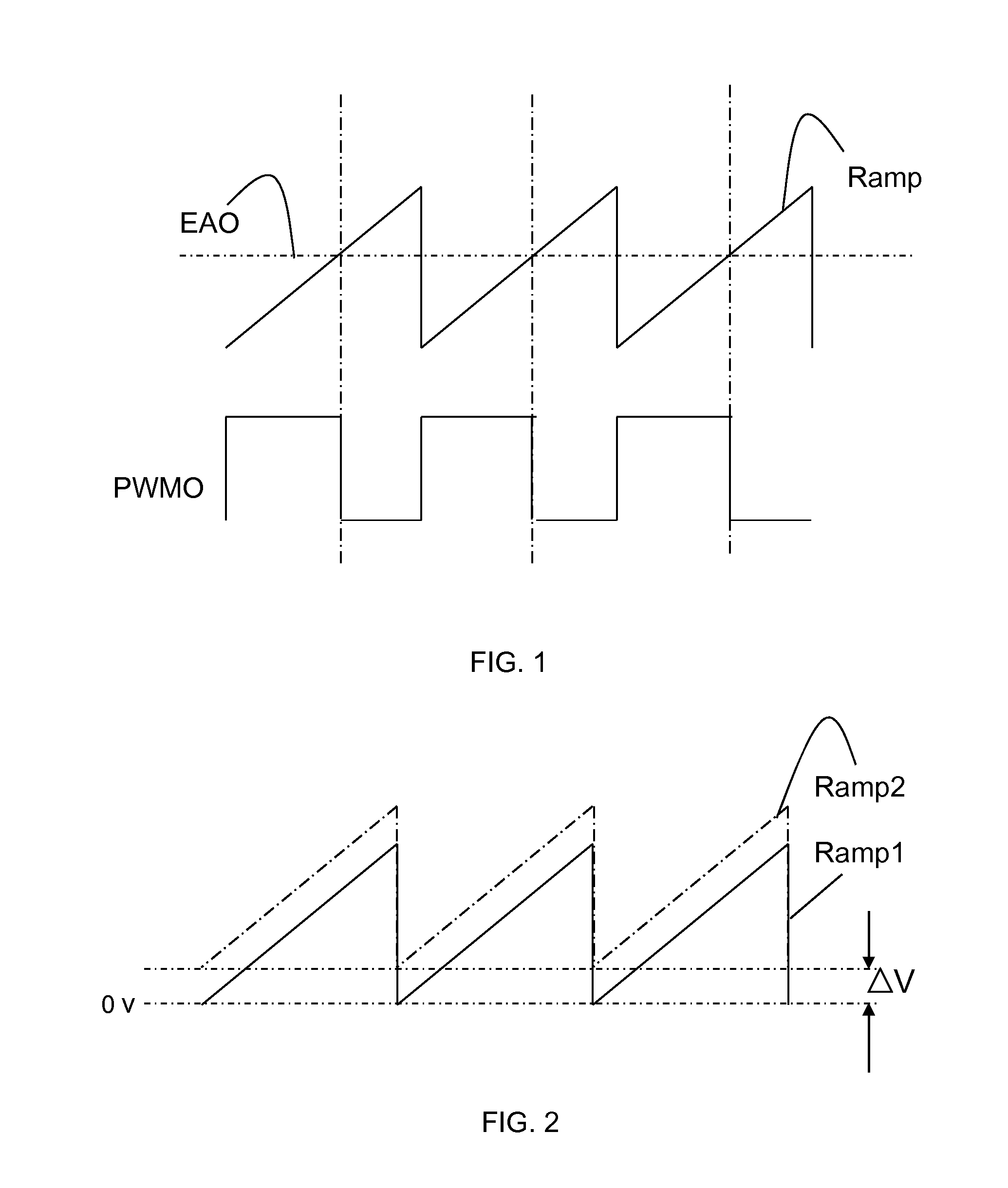
[0038]FIG. 5A is a schematic circuit diagram showing a first exemplary configuration of a multiple-input comparator 500 according to the present invention. Referring to FIG. 5A, the multiple-input comparator 500 comprises a differential transistor pair (MP51 and MP52), a first resistor R51, a second resistor R52 and a current source I51. The length-to-width ratio of the first differential transistor MP51 is equal to that of the second differential transistor MP52.

[0039]The first differential transistor MP51 is a PMOS transistor. The gate of the first differential transistor MP51 is used as the first voltage input terminal of the multiple-input comparator 500 to receive the error amplifying voltage EAO. The second differential transistor MP52 is also a PMOS transistor. The gate of the second differential transistor MP52 is used as the second voltage input terminal of the multiple-input comparator 500 to receive the voltage Ramp. One terminal of the first resistor R51 is connected to ...

second embodiment

[0053]FIG. 6A is a schematic circuit diagram showing a first exemplary configuration of a multiple-input comparator 600 according to the present invention. Referring to FIGS. 6A, 5A and 5B, comparing the multiple-input comparator 500 shown in FIG. 5A and FIG. 5B, the multiple-input comparator 600 further comprises a first differential transistor MP61, a second differential transistor MP62 to form a differential transistor pair, a first resistor R61, a second resistor R62 and a current source I61. A connection relationship of the electric elements above mentioned is identical with that shown in FIG. 5A and FIG. 5B, which is omitted herein for simplicity. In one embodiment, a node INJ1 between the first resistor R61 and the first differential transistor MP61 is used as the current input terminal to connect to a current source. In another embodiment, a node INJ2 between the second resistor R62 and the second differential transistor MP62 is used as the current input terminal to connect ...

third embodiment

[0057]FIG. 7 is a schematic circuit diagram showing a multiple-input comparator 700 according to the present invention. Referring to FIG. 7 and FIG. 6A, comparing to the multiple-input comparator 600, the multiple-input comparator 700 further comprises a first differential transistor MP71, a second differential transistor MP72 forming a differential transistor pair together with a first differential transistor MP71, a first resistor R71, a second resistor R72 and a current source I71. A connection relationship of the electric elements above mentioned is identical with that shown in FIG. 6A, which is omitted herein for simplicity. In one embodiment, a node INJ1 between the first resistor R71 and the first differential transistor MP71 is used as the current input terminal to connect to a current source. In another embodiment, a node INJ2 between the second resistor R72 and the second differential transistor MP72 is used as the current input terminal to connect to a current sink.

[0058]...


PUM


Abstract

Techniques pertaining to multiple-input comparator and power converter designs are disclosed. According to one aspect, the present invention discloses a multiple-input comparator comprising a pair of differential transistors connected by a resister. The gate terminals of the transistor pair serve as the input terminals of the comparator for receiving external voltage for comparison. The terminal of the resistor serves as the current input terminal and is either connected to a current source or a current sink. A power inverter utilizing the multiple-input comparator is also disclosed. The power inverter comprises a power switch driven by a PMW signal, a voltage sampling circuit, an error amplifier and a multiple-input PWM comparator.

Description

BACKGROUND OF THE INVENTION[0001]1. Field of the Invention[0002]The present invention relates to a field of circuit design, more particularly to multiple-input comparator and power converter circuits.[0003]2. Description of Related Art[0004]In the prior art, a pulse width modulation system usually employs a pulse width modulation (PWM) comparator. FIG. 1 is a schematic diagram showing a comparison principle of the PWM comparator. EAO is an error amplifying (output) signal outputted from an error amplifier. Ramp is a saw-tooth or triangular wave signal. The PWM comparator is provided for comparing an error amplifying signal EAO with the triangular wave signal Ramp to produce a pulse width modulation (output) signal PWMO. When the error amplifying signal EAO is larger than the triangular wave signal Ramp, the PWM signal PWMO is set at high level. When the error amplifying signal EAO is smaller than the triangular wave signal Ramp, the PWM signal PWMO is set at low level. In other word...

Claims


Application Information

Patent Timeline
Patent Type & Authority Applications(United States)
IPC IPC(8): G05F1/10H03F3/45
CPCH03F2200/351H03F2200/78H03K5/2481H03F2203/45392H03F2203/45374
Inventor WANG, ZHAODONG, XIANHUIYANG, DAVE XIAODONG
Owner WUXI ZGMICRO ELECTRONICS CO LTD
Why Eureka
Try Eureka