Connecting material, method for manufacturing connecting material and semiconductor device

a technology of connecting material and manufacturing method, which is applied in the direction of manufacturing tools, soldering apparatus, and semiconductor/solid-state device details, etc., can solve the problems of insufficient wetness, inability to suppress temperature cycle, and breakage of semiconductor elements due to thermal stress at the cooling time of connection or after connection cooling, etc., to improve connection reliability, reduce the process of manufacturing material, and improve the wetness at the time of connection

Active Publication Date: 2012-01-05
HITACHI LTD
View PDF8 Cites 4 Cited by
  • Summary
  • Abstract
  • Description
  • Claims
  • Application Information

AI Technical Summary

Benefits of technology

[0011]In consideration of these points, an object of the present invention is to provide a connecting material capable of applying a Zn—Al series alloy having a melting point of 260° C. or higher to the connection, improving the wetness at the time of connection, reducing the processes for manufacturing the material and improving the connection reliability for the thermal stress.

Problems solved by technology

That is, since Al is contained in a Zn—Al series alloy, sufficient wetness cannot be ensured.
Further, the breakage of a semiconductor element due to the thermal stress at the time of cooling after the connection or in the temperature cycle cannot be suppressed.

Method used


Image

  • Connecting material, method for manufacturing connecting material and semiconductor device
  • Connecting material, method for manufacturing connecting material and semiconductor device
  • Connecting material, method for manufacturing connecting material and semiconductor device

Examples


embodiment

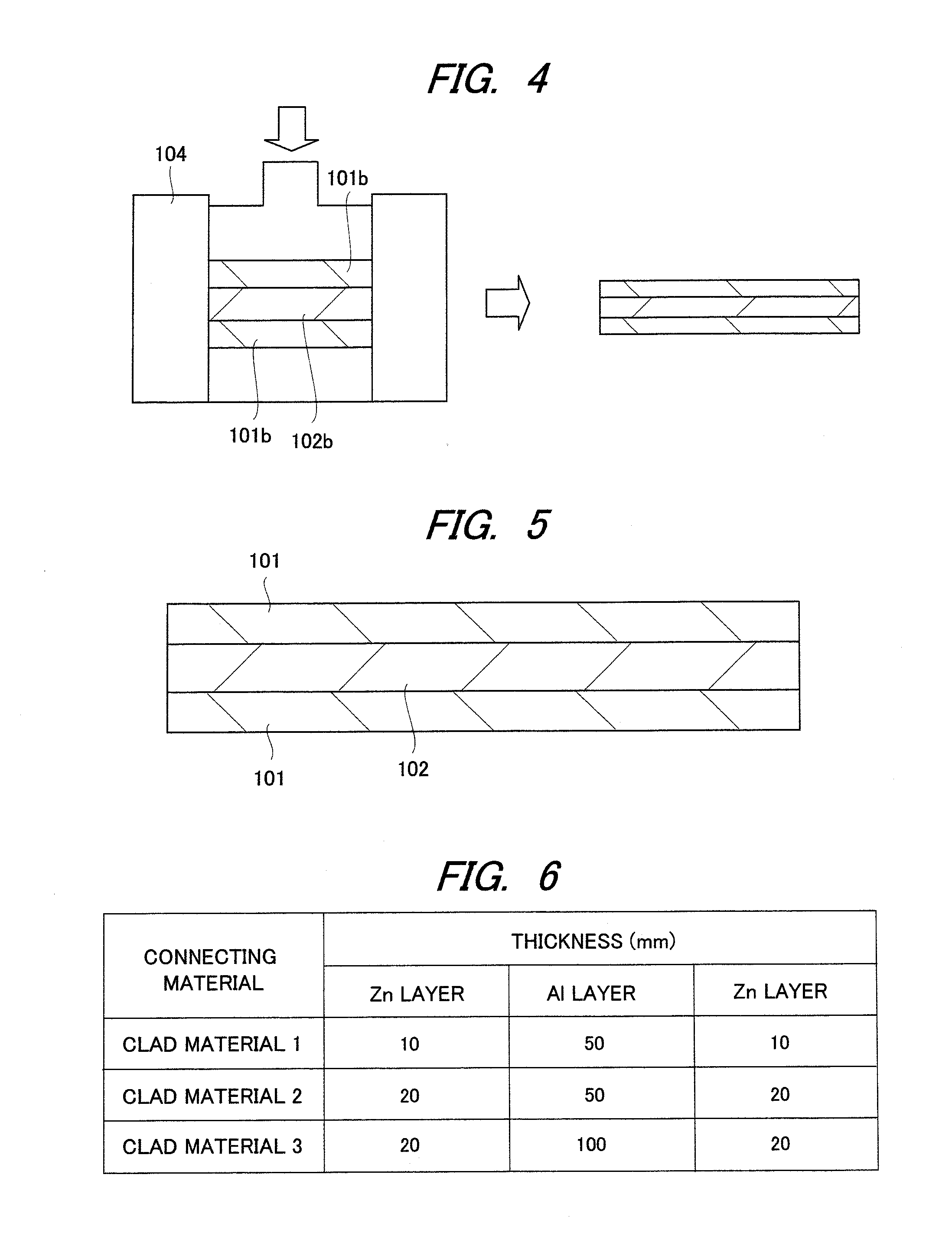
[0038]FIG. 5 shows a cross section of a connecting material according to the embodiment of the present invention. In the connecting material according to the present embodiment, a Zn series alloy layer (simply referred to as Zn layer or Zn) 101 as a lower layer, an Al series alloy layer (simply referred to as Al layer or Al) 102 as an intermediate layer and a Zn series alloy layer (simply referred to as Zn layer or Zn) 101 as an upper layer are formed. As shown in FIG. 3 described above, this connecting material is manufactured by stacking the Zn series alloy layer 101a, the Al series alloy layer 102a and the Zn series alloy layer 101a and then performing the rolling process, that is, the clad rolling.

[0039]FIG. 6 shows all the connecting materials (referred to as clad material) thus manufactured. In the clad material 1, the thicknesses of the Zn layer, the Al layer and the Zn layer are 10, 50 and 10 μm, respectively. In the clad material 2, the thicknesses thereof are 20, 50 and 20...

examples 1 to 12

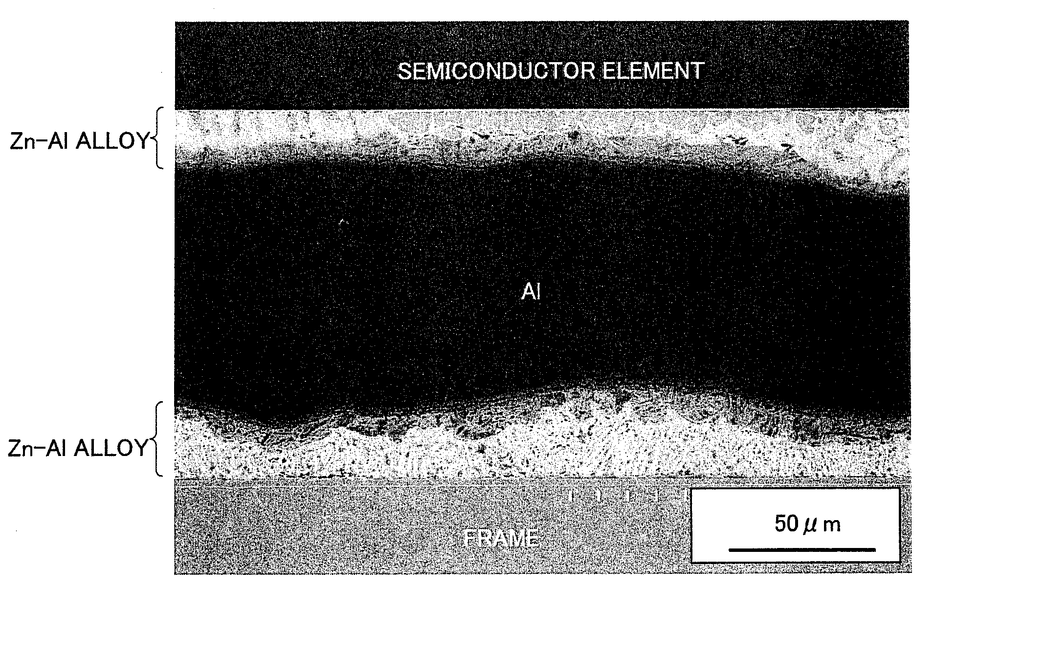
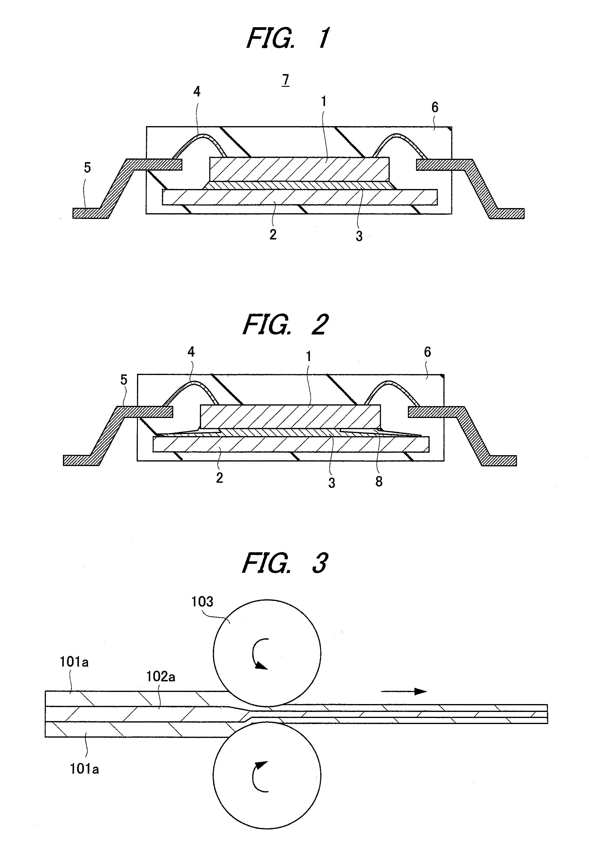
[0040]In the examples 1 to 12, as shown in FIG. 7, the connecting material 10 is used for the die bonding of the semiconductor device 11. This semiconductor device 11 includes a semiconductor element 1, a frame 2 connecting the semiconductor element 1, a lead 5 whose one end functions as an external terminal, a wire 4 connecting the other end of the lead 5 and an electrode of the semiconductor element 1, and a sealing resin 6 which seals the semiconductor element 1 and the wire 4, and the semiconductor element 1 and the frame 2 are connected by the connecting material 10.

[0041]In the manufacture of the semiconductor device 11, the connecting material 10 is supplied onto the frame 2 made of solid Cu or the frame 2 on which the Ni, Ni / Ag or Ni / Au plating is performed and the semiconductor element 1 is placed thereon, and thereafter, the heating is performed at 400° C. for 1 min. in an N2 atmosphere while applying pressure, whereby the semiconductor element 1 is die-bonded. FIG. 8 show...

examples 13 to 24

[0046]In the examples 13 to 24, as shown in FIG. 10, the connecting material 10a of the present invention is used as the sealing material of a semiconductor device 21 requiring the hermetic sealing. This semiconductor device 21 includes a semiconductor element 1, a module substrate 23 connecting the semiconductor element 1, a lead 5 whose one end functions as an external terminal, a wire 4 connecting the other end of the lead 5 and an electrode of the semiconductor element 1, and a metal cap 22 which hermetically seals the semiconductor element 1 and the wire 4 and is connected to the module substrate 23, and the module substrate 23 and the metal cap 22 are connected by the connecting material 10a. Note that, in the semiconductor device 21, chip components and others are also connected onto the module substrate 23.

[0047]In the manufacture of the semiconductor device 21, after the semiconductor element 1, the chip components and others are connected to the module substrate 23 by an S...


PUM

PropertyMeasurementUnit
offset yield strengthaaaaaaaaaa
melting pointaaaaaaaaaa

Abstract

In a connecting material of the present invention, a Zn series alloy layer is formed on an outermost surface of an Al series alloy layer. In particular, in the connecting material, anAl content of the Al series alloy layer is 99 to 100 wt. % or a Zn content of the Zn series alloy layer is 90 to 100 wt. %. By using this connecting material, the formation of an Al oxide film on the surface of the connecting material at the time of the connection can be suppressed, and preferable wetness that cannot be obtained with the Zn—Al alloy can be obtained. Further, when an Al series alloy layer is left after the connection, since the soft Al functions as a stress buffer material, the high connection reliability can be achieved.

Description

CROSS-REFERENCE TO RELATED APPLICATION[0001]The present application claims priority from Japanese Patent Application No. JP 2006-314168 filed on Nov. 21, 2006, the content of which is hereby incorporated by reference into this application.[0002]This application is a Divisional application of Application No. 11 / 943,632, filed No. 21, 2007, the contents of which are incorporated herein by reference in their entirety.TECHNICAL FIELD OF THE INVENTION[0003]The present invention relates to a technology for a connecting material. More particularly, the present invention relates to a technology effectively applied to a structure and a manufacturing method of the connecting material, and a semiconductor device, a power semiconductor device and a power module using the connecting material.BACKGROUND OF THE INVENTION[0004]As a technology that the inventors of the present invention have been examined, a semiconductor device using a connecting material will be described with reference to FIG. 1 ...

Claims


Application Information

Patent Timeline
Patent Type & Authority Applications(United States)
IPC IPC(8): H01L21/00B23K31/00
CPCB23K20/02B23K20/04B32B15/017H01L24/27H01L24/32H01L24/48H01L24/743H01L24/83H01L2224/32245H01L2224/48091H01L2224/48137H01L2224/48247H01L2224/73265H01L2224/83101H01L2224/83801H01L2924/01009H01L2924/01012H01L2924/01013H01L2924/01015H01L2924/01027H01L2924/01029H01L2924/0103H01L2924/01032H01L2924/01033H01L2924/01047H01L2924/0105H01L2924/01074H01L2924/01075H01L2924/01078H01L2924/01079H01L2924/01082H01L2924/01322H01L2924/13055H01L2924/01006H01L2924/014H01L2924/0132H01L24/29H01L2224/83805H01L2224/29111H01L2924/0133H01L2224/32225H01L2224/291H01L2224/83455H01L2924/15747B23K35/0238H01L23/49582Y10T428/12736H01L2924/00014H01L2924/01014H01L2924/00H01L2924/00012H01L2924/01083H01L2924/3512H01L2924/351H01L24/73H01L2924/181Y10T428/31678H01L2224/2612H01L2224/45099H01L2224/05599H01L23/48
Inventor IKEDA, OSAMUOKAMOTO, MASAHIDE
Owner HITACHI LTD
Why Eureka
Try Eureka