Supercharge Your Innovation With Domain-Expert AI Agents!

SRAM with buffered-read bit cells and its testing

a bit cell and buffered-read technology, applied in static storage, information storage, digital storage, etc., can solve the problems of affecting product yield, pfa is time-consuming, destructive, and may not reveal

Active Publication Date: 2012-01-19
TEXAS INSTR INC
View PDF7 Cites 5 Cited by
  • Summary
  • Abstract
  • Description
  • Claims
  • Application Information

AI Technical Summary

Problems solved by technology

Shrinking semiconductor integrated circuit feature sizes have placed increasing challenges on semiconductor integrated circuit processing.
As a result, subtle defects at these minimum feature sizes can adversely impact product yield.
However, PFA is time consuming, destructive, and may not reveal all defects such as gate dielectric failure.
Additional complexity of current memory cells such as the 8T SRAM memory cell disclosed by Chang et al., “Stable SRAM Cell Design for the 32 nm Node and Beyond,” 2005 Symposium on VLSI Technology, 8A-2, 128 (2005), further complicate PFA.
Moreover, the 8T SRAM cell of Chang et al. further complicates characterization of individual memory cells in a functional memory circuit.

Method used


Image

  • SRAM with buffered-read bit cells and its testing
  • SRAM with buffered-read bit cells and its testing
  • SRAM with buffered-read bit cells and its testing

Examples


Embodiment Construction

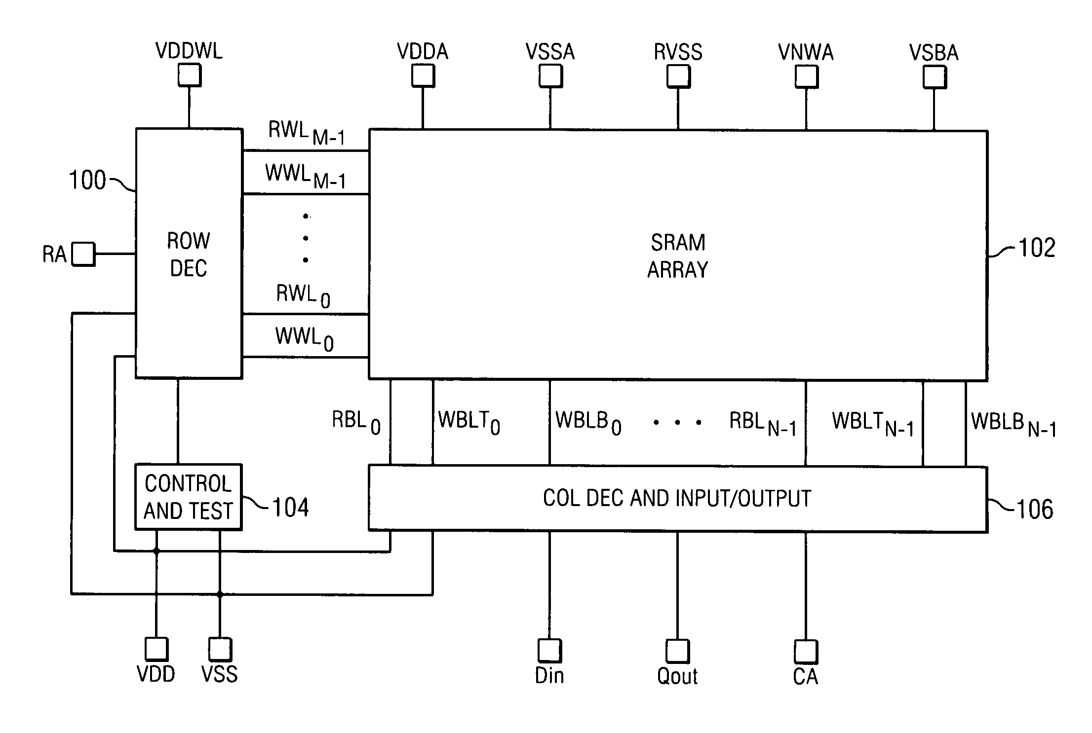
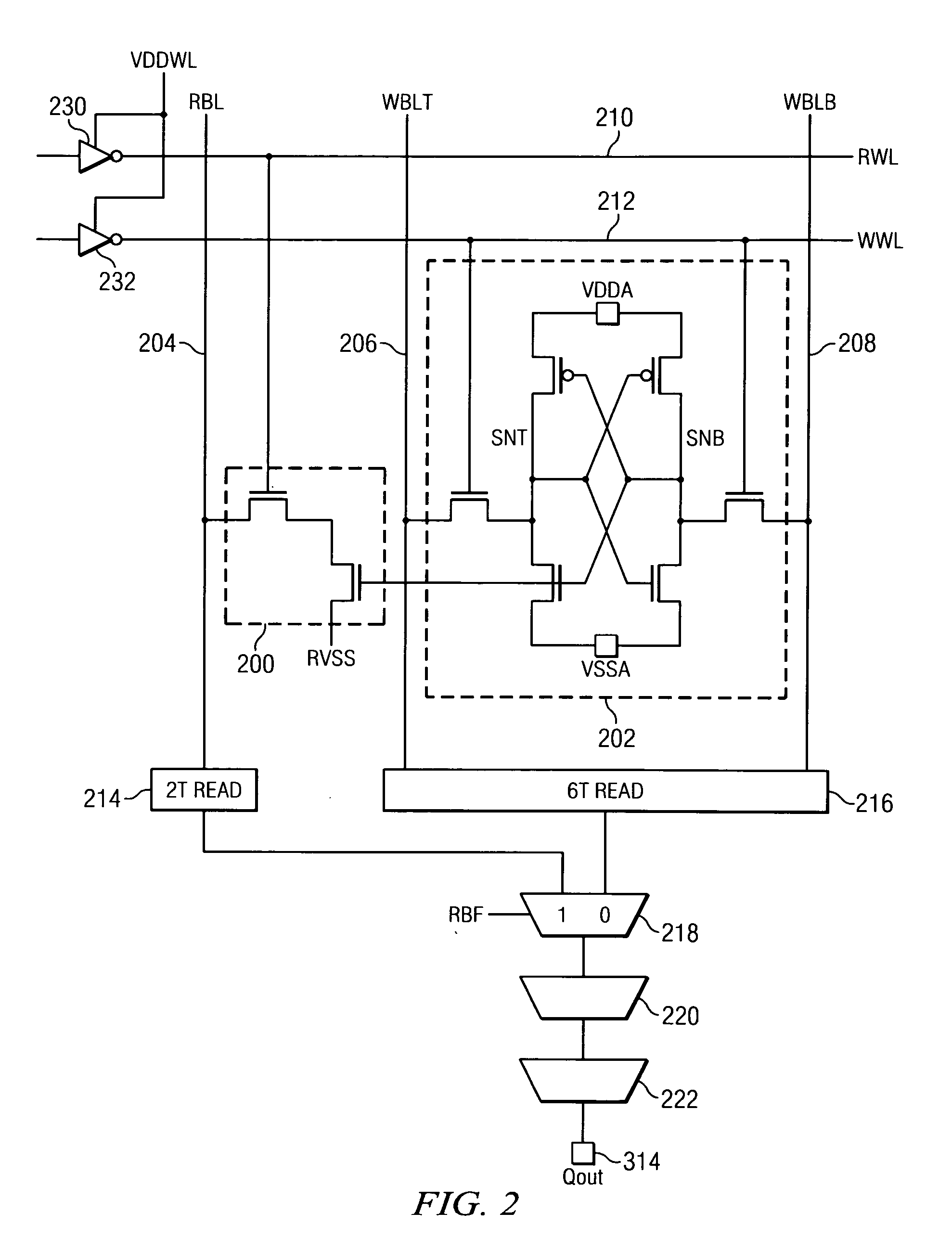
[0015]The preferred embodiments of the present invention provide significant advantages in electrical failure analysis and characterization of individual buffered-read memory cells or individual transistors of buffered-read memory cells of a functional static random access memory (SRAM) using functional test or direct bit line access (DBLA).

[0016]The present inventors have previously disclosed a circuit and method to characterize individual transistors of a 6-transistor (6T) SRAM memory cell by direct bit line access in application Ser. No. 12 / 347,928, filed Dec. 31, 2008, and incorporated herein by reference in its entirety. Additional disclosures by the present inventors regarding characterization of individual transistors of a 6T SRAM memory cell are also presented at Deng et al., “Characterization of Bit Transistors in a Functional SRAM,” 2008 Symposium on VLSI Technology, 44 (2008) and Deng et al., “Measurement of Bit Leakages in a Functional SRAM,” 2009 Proceedings from the 35...


PUM


Abstract

An SRAM with buffered-read bit cells is disclosed (FIGS. 1-6). The integrated circuit includes a plurality of memory cells (102). Each memory cell has a plurality of transistors (200, 202). A first memory cell (FIG. 2) is arranged to store a data signal in response to an active write word line (WWL) and to produce the data signal in response to an active read word line (RWL). A test circuit (104) formed on the integrated circuit is operable to test current and voltage characteristics of each transistor of the plurality of transistors of the first memory cell (FIGS. 7-10).

Description

CLAIM TO PRIORITY OF NONPROVISIONAL APPLICATION[0001]This application claims the benefit under 35 U.S.C. §119(e) of Provisional Appl. No. 61 / 365,157 (TI-69533PS), filed Jul. 16, 2010, which is incorporated herein by reference in its entirety.BACKGROUND OF THE INVENTION[0002]Embodiments of the present invention relate to a static random access memory (SRAM), particularly an SRAM with buffered-read bit cells and its testing.[0003]Shrinking semiconductor integrated circuit feature sizes have placed increasing challenges on semiconductor integrated circuit processing. In particular, a balance between high packing density and yield requires a finely tuned manufacturing process. Minimum feature sizes of high density memory cells are frequently less than corresponding feature sizes of peripheral circuits. As a result, subtle defects at these minimum feature sizes can adversely impact product yield. Physical failure analysis (PFA) has often been used to determine the precise cause of these ...

Claims


Application Information

Patent Timeline
IPC IPC(8): G11C7/00
CPCG11C11/41G11C11/419G11C29/022G11C8/16
Inventor DENG, XIAOWEILOH, WAH KIT
Owner TEXAS INSTR INC
Features
  • R&D
  • Intellectual Property
  • Life Sciences
  • Materials
  • Tech Scout
  • Unparalleled Data Quality
  • Higher Quality Content
  • 60% Fewer Hallucinations
Learn More