Ceramic electronic component and wiring board

a technology of electronic components and wiring boards, applied in the direction of fixed capacitor details, semiconductor/solid-state device details, fixed capacitors, etc., can solve the problems of reducing the overall reliability of the wiring board, affecting the treatment effect, and affecting the effect of the treatment effect, etc., to achieve the effect of preventing the entry of treatment liquid, high adhesion strength, and reliable bonding

Active Publication Date: 2012-01-26
MURATA MFG CO LTD
View PDF10 Cites 38 Cited by
  • Summary
  • Abstract
  • Description
  • Claims
  • Application Information

AI Technical Summary

Benefits of technology

[0009]To overcome the problems described above, preferred embodiments of the present invention provide a ceramic electronic component that improves the reliability of a ceramic-electronic-component embedded wiring board.
[0015]In various preferred embodiments of the present invention, since the projecting portions of the external electrodes project more than the other portions in the thickness direction, when the ceramic electronic component is bonded on the base substrate with the adhesive, a space in which the adhesive enters is ensured between the external electrodes and the base substrate. This enables reliable bonding with high adhesion strength. For this reason, it is possible to prevent entry of treatment liquid between the external electrodes and the base substrate. Therefore, high reliability is achieved.

Problems solved by technology

However, when the chip capacitor is embedded in the wiring board, as in Japanese Unexamined Patent Application Publication No. 2001-352141, the overall reliability of the wiring board decreases.
However, since the entire wraparound portion of an external electrode contacts the base substrate, the adhesive does not properly enter between the external electrode and the base substrate, and the thickness of a layer of the adhesive becomes too small between the external electrode and the base substrate.
This decreases the adhesion strength and the adhesive is not provided.
This solution reduces reliability.

Method used


Image

  • Ceramic electronic component and wiring board
  • Ceramic electronic component and wiring board
  • Ceramic electronic component and wiring board

Examples


first preferred embodiment

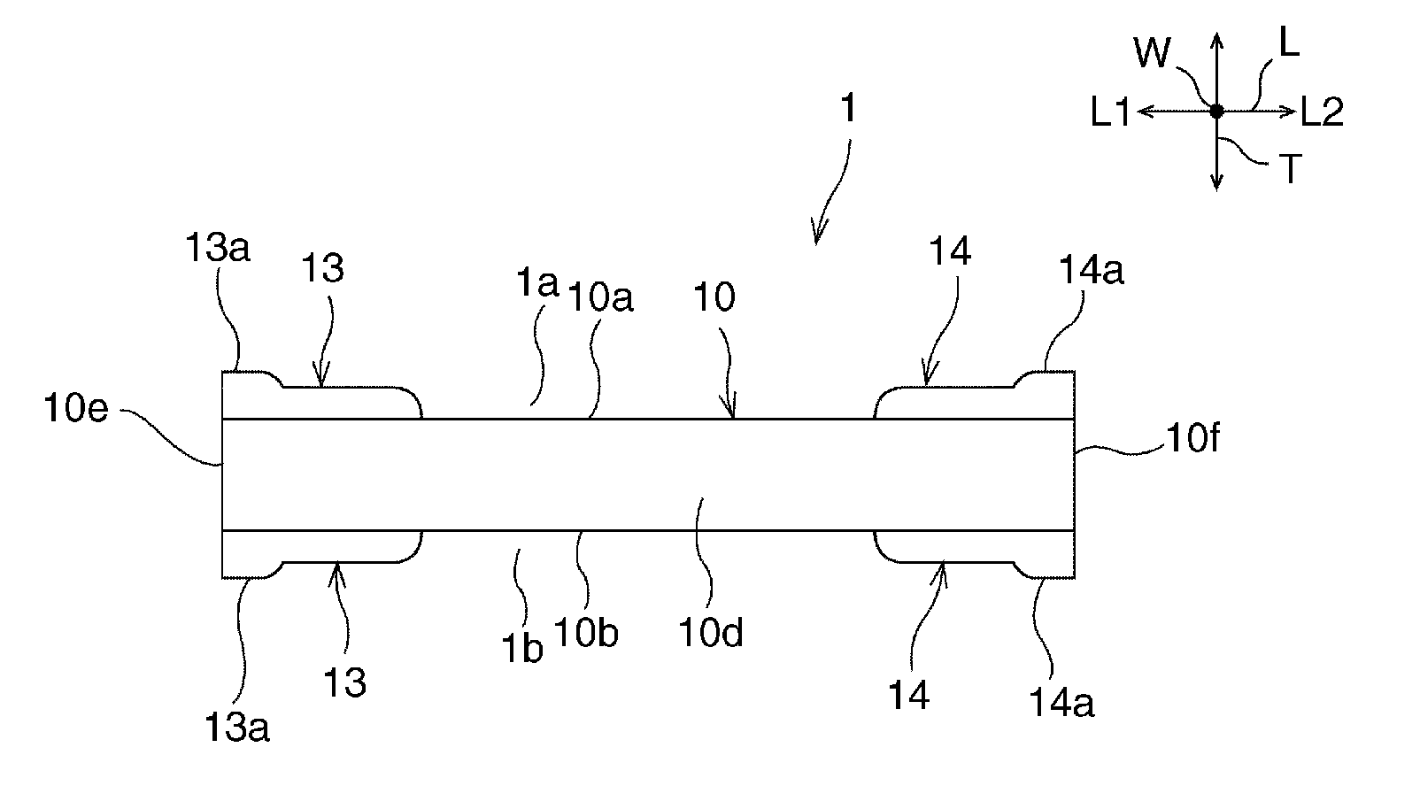
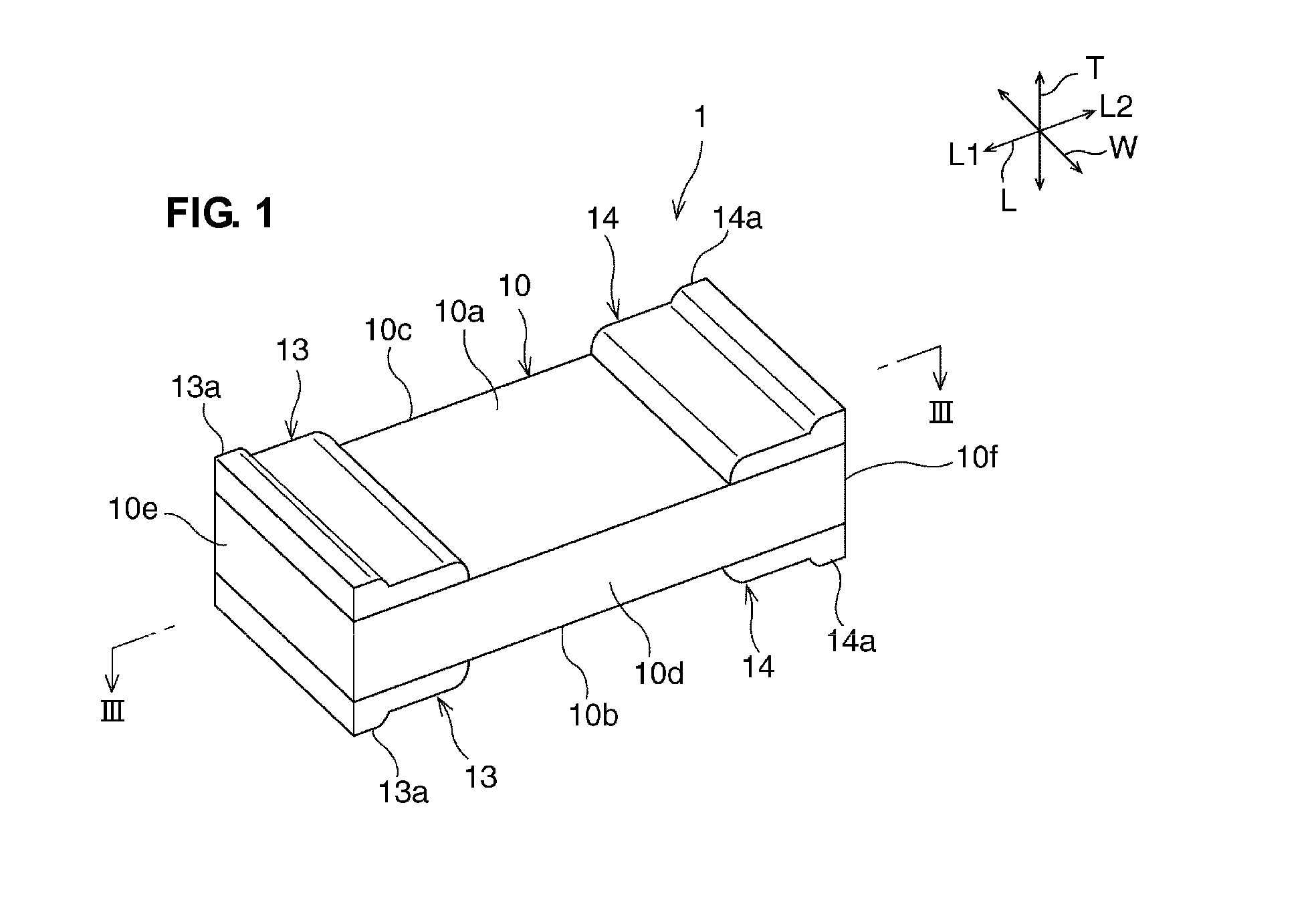
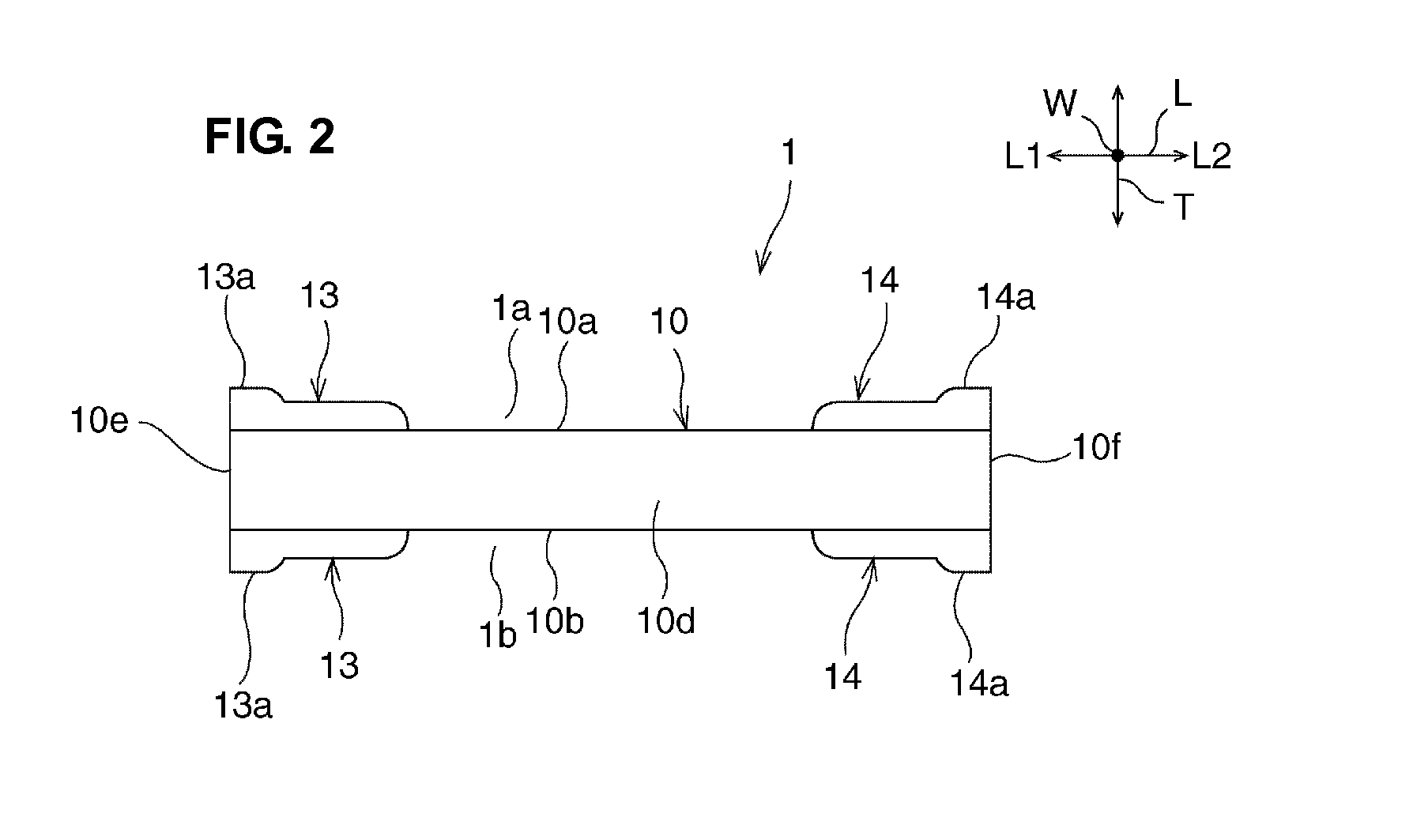
[0032]A first preferred embodiment of the present invention will be described below by taking a ceramic electronic component 1 illustrated in FIG. 1, as an example. The ceramic electronic component 1 is just exemplary, and the ceramic electronic component according to preferred embodiments of the present invention is not limited thereto.

[0033]FIG. 1 is a schematic perspective view of the ceramic electronic component 1 of the first preferred embodiment. FIG. 2 is a schematic side view of the ceramic electronic component 1. FIG. 3 is a schematic cross-sectional view, taken along line III-III of FIG. 1. FIG. 4 is a schematic sectional view taken along line IV-IV of FIG. 3. FIG. 5 is a schematic sectional view taken along line V-V of FIG. 3.

[0034]First, the structure of the ceramic electronic component 1 will be described with reference to FIGS. 1 to 5.

[0035]As illustrated in FIGS. 1 to 5, the ceramic electronic component 1 preferably includes a ceramic element body 10. The ceramic elem...


PUM

PropertyMeasurementUnit
thicknessaaaaaaaaaa
thicknessaaaaaaaaaa
thicknessaaaaaaaaaa

Abstract

A ceramic electronic component includes a ceramic element body having a substantially rectangular parallelepiped shape, and first and second external electrodes. The first and second external electrodes are provided on a first principal surface. Portions of the first and second external electrodes project further than the other portions in a thickness direction. A projecting portion of the first external electrode is provided at one end of the first external electrode in a length direction and a second projecting portion of the second external electrode is provided at another end of the second external electrode in the length direction. Thus, a concave portion is provided between the projecting portions, and a portion of the first principal surface provided between the first and second external electrodes is exposed.

Description

BACKGROUND OF THE INVENTION[0001]1. Field of the Invention[0002]The present invention relates to a ceramic electronic component and a wiring board. More particularly, the present invention relates to a ceramic electronic component suitably used while being embedded in a wiring board, and to a ceramic-electronic-component embedded wiring board in which the ceramic electronic component is embedded.[0003]2. Description of the Related Art[0004]With recent reduction in size and thickness of electronic apparatuses, such as mobile telephones and portable music players, the sizes of wiring boards to be mounted in the electronic apparatuses have been reduced.[0005]For example, Japanese Unexamined Patent Application Publication No. 2001-352141 discloses a method for reducing the size of a wiring board, in which a chip capacitor is embedded in a wiring board, a through hole is formed in a portion of the wiring board above the chip capacitor with a laser, and the inside of the through hole is p...

Claims


Application Information

Patent Timeline
Patent Type & Authority Applications(United States)
IPC IPC(8): H05K1/16H01L41/00H01C7/13H01G4/12H01F5/00H01G4/232H01G4/30H05K3/46
CPCH01G4/232H01G4/236H01G4/30H01L23/49822H01L23/50H05K1/185H01L2924/0002H05K2201/10015H05K2203/1469H01L2924/00H01G4/12H05K3/46
Inventor SATO, KOJISANADA, YUKIONISHISAKA, YASUHIRO
Owner MURATA MFG CO LTD
Why Eureka
Try Eureka