Semiconductor device and method for manufacturing the same

a semiconductor and semiconductor technology, applied in the direction of semiconductor devices, electrical equipment, transistors, etc., can solve the problems of reducing the reliability of transistors including oxide semiconductors, and achieve the effects of stable electrical characteristics, low cost and high reliability

Active Publication Date: 2012-01-26
SEMICON ENERGY LAB CO LTD
View PDF0 Cites 64 Cited by
  • Summary
  • Abstract
  • Description
  • Claims
  • Application Information

AI Technical Summary

Benefits of technology

[0040]According to one embodiment of the present invention, an insulating layer from which oxygen is released by heating is provided as an insulating layer in contact with a channel region of an oxide semiconductor layer, and an insulating layer which releases a smaller amount of oxygen than the insulating layer in contact with the channel region is provided as an insulating layer in contact with a source region and a drain region of the oxide semiconductor layer. As a result, a transistor having a small off-state current, small variation in the threshold voltage, a large on-state current, and stable electrical characteristics can be provided.
[0041]According to one embodiment of the present invention, a semiconductor device including a highly reliable transistor having favorable electric characteristics is provided.

Problems solved by technology

Fluctuation in the threshold voltage due to a BT test of the transistor including an oxide semiconductor remarkably reduces the reliability of the transistor including an oxide semiconductor.

Method used


Image

  • Semiconductor device and method for manufacturing the same
  • Semiconductor device and method for manufacturing the same
  • Semiconductor device and method for manufacturing the same

Examples


embodiment 1

[0054]In this embodiment, an embodiment of a semiconductor device and a method for manufacturing the semiconductor device will be described with reference to FIGS. 1A and 1B, FIGS. 2A to 2D, FIGS. 3A to 3D, FIGS. 4A to 4D, and FIGS. 5A and 5B.

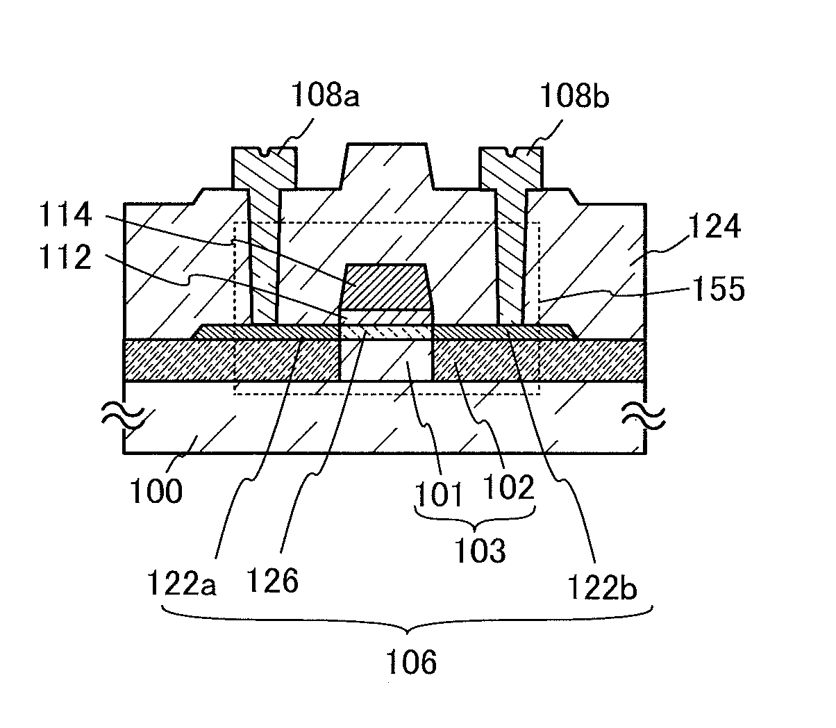
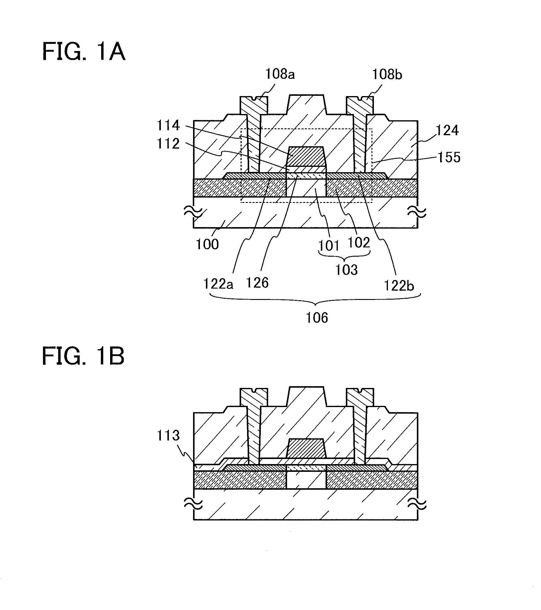
[0055]FIGS. 1A and 1B each illustrate a cross-sectional view of a coplanar transistor 155, which is one mode of a top-gate transistor, as an example of a semiconductor device according to an embodiment of the present invention.

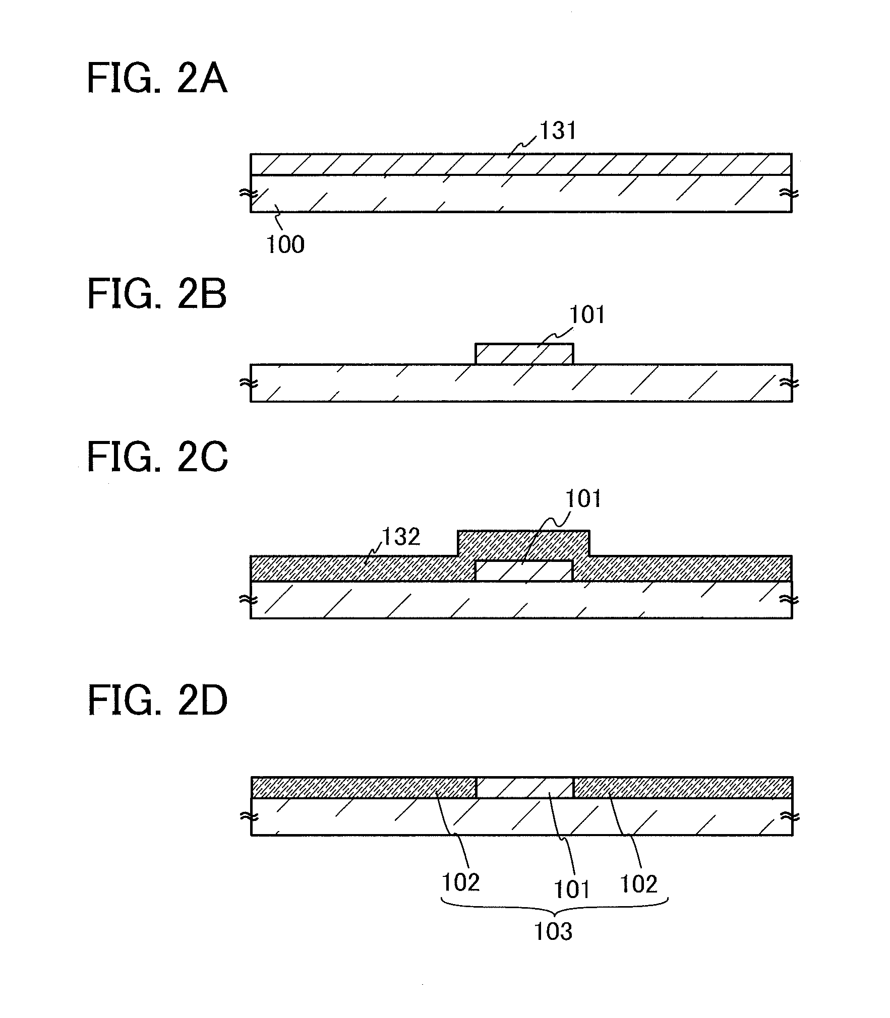
[0056]The transistor 155 illustrated in FIG. 1A includes an insulating layer 103, an oxide semiconductor layer 106, a gate insulating layer 112, and a gate electrode 114, which are over a substrate 100. The insulating layer 103 includes a first region 101 and a second region 102. The oxide semiconductor layer 106 of the transistor 155 includes a channel region 126, a source region 122a, and a drain region 122b. The channel region 126, the source region 122a, and the drain region 122b are included in the same layer.

[0057]T...

embodiment 2

[0140]In this embodiment, an embodiment of a semiconductor device will be described with reference to FIG. 6. FIG. 6 illustrates a cross section of a transistor 156 having a structure which is different from that of the transistor 155 illustrated in FIG. 1A. The transistor 156 illustrated in FIG. 6 is different from the transistor 155 illustrated in FIG. 1A in that the second region 102 is not provided.

[0141]The transistor 156 in FIG. 6 includes a first insulating layer 104, an oxide semiconductor layer 106, a gate insulating layer 112, and a gate electrode 114, which are over a substrate 100. The transistor 156 includes, in the oxide semiconductor layer 106, a channel region 126, a source region 122a, and a drain region 122b. The channel region 126, the source region 122a, and the drain region 122b are provided in the same layer.

[0142]A second insulating layer 105 may be provided below the transistor 156. The second insulating layer 105 functions as a base layer of the transistor 1...

embodiment 3

[0161]In this embodiment, an embodiment of a semiconductor device will be described with reference to FIGS. 9A to 9C. FIG. 9A is a top view of a transistor. FIG. 9B illustrates a cross-sectional structure corresponding to an alternate long and short dashed line A-B in FIG. 9A.

[0162]A transistor illustrated in FIG. 9B includes an insulating layer 103, an oxide semiconductor layer 136, a gate insulating layer 112, a gate electrode 114, a sidewall insulating layer 130, a source electrode 116a, and a drain electrode 116b over a substrate 100. The insulating layer 103 includes a first region 101 and a second region 102. The transistor illustrated in FIG. 9B includes a channel region 126, a source region 122a, a drain region 122b, an offset region 123a, and an offset region 123b in the oxide semiconductor layer 136. The channel region 126, the source region 122a, the drain region 122b, the offset region 123a, and the offset region 123b are provided in the same layer.

[0163]The offset regio...


PUM


Abstract

An insulating layer which releases a large amount of oxygen is used as an insulating layer in contact with a channel region of an oxide semiconductor layer, and an insulating layer which releases a small amount of oxygen is used as an insulating layer in contact with a source region and a drain region of the oxide semiconductor layer. By releasing oxygen from the insulating layer which releases a large amount of oxygen, oxygen deficiency in the channel region and an interface state density between the insulating layer and the channel region can be reduced, so that a highly reliable semiconductor device having small variation in electrical characteristics can be manufactured. The source region and the drain region are provided in contact with the insulating layer which releases a small amount of oxygen, thereby suppressing the increase of the resistance of the source region and the drain region.

Description

BACKGROUND OF THE INVENTION[0001]1. Field of the Invention[0002]The present invention relates to a semiconductor device and a method for manufacturing the semiconductor device.[0003]In this specification, a semiconductor device means a general device which can function by utilizing semiconductor characteristics, and an electro-optic device, a semiconductor circuit, and an electronic device are all semiconductor devices.[0004]2. Description of the Related Art[0005]A technique by which transistors are formed using semiconductor thin films over a substrate having an insulating surface has been attracting attention. Such transistors are applied to a wide range of electronic devices such as integrated circuits (ICs) or image display devices (display devices). A silicon-based semiconductor material is widely known as a material for a semiconductor thin film applicable to a transistor. As another material, an oxide semiconductor has been attracting attention.[0006]For example, a transistor...

Claims


Application Information

Patent Timeline
Patent Type & Authority Applications(United States)
IPC IPC(8): H01L29/786H01L21/336
CPCH01L29/66742H01L29/78603H01L29/78618H01L29/66969H01L21/02164H01L21/02367H01L21/02565H01L29/7869H01L21/02631H01L29/78696
Inventor ENDO, YUTANODA, KOSEISASAKI, TOSHINARI
Owner SEMICON ENERGY LAB CO LTD
Why Eureka
Try Eureka