

Ceramic electronic component
a technology of ceramic electronic components and components, applied in the direction of fixed capacitor details, generators/motors, fixed capacitors, etc., can solve the problems of reducing and achieve the effect of increasing the reliability of ceramic electronic components and reducing thickness
- Summary
- Abstract
- Description
- Claims
- Application Information
AI Technical Summary
Benefits of technology
Problems solved by technology
Method used
Image

Examples
first preferred embodiment
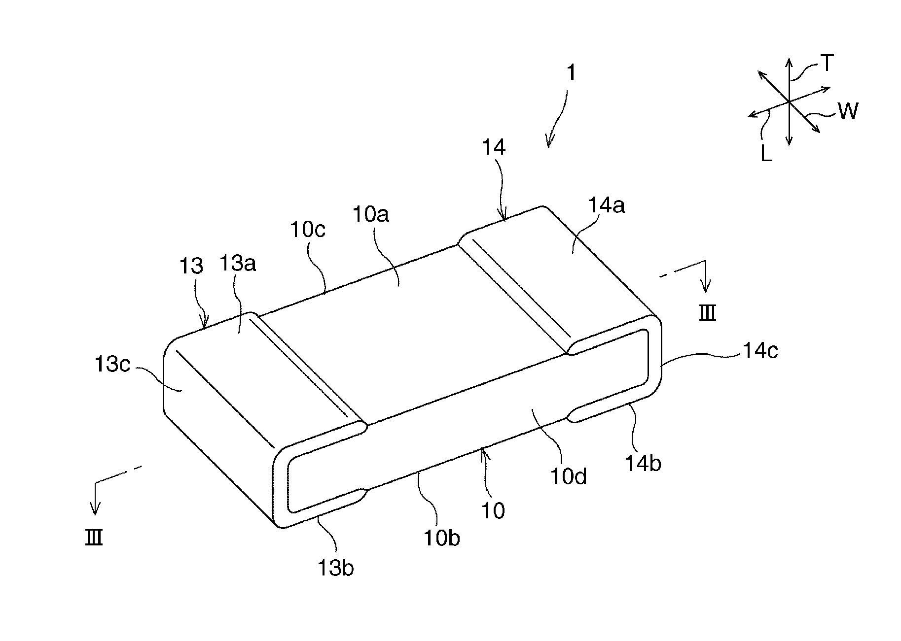
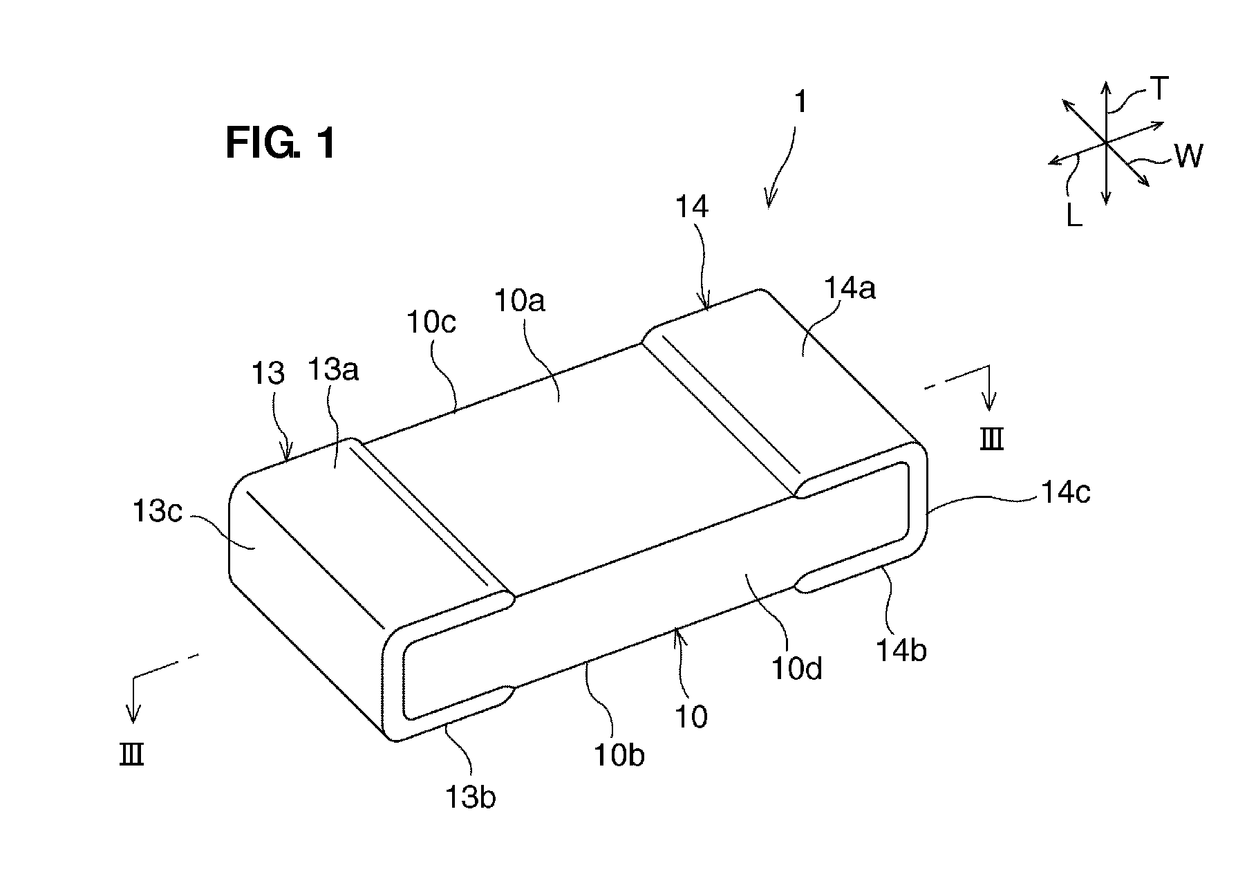
[0024]A preferred embodiment of the present invention is described below using a ceramic electronic component 1 illustrated in FIG. 1 as an example. The ceramic electronic component 1 is merely an example of a preferred embodiment of the present invention. The present invention is not limited to the ceramic electronic component 1 and a method of producing it described below.
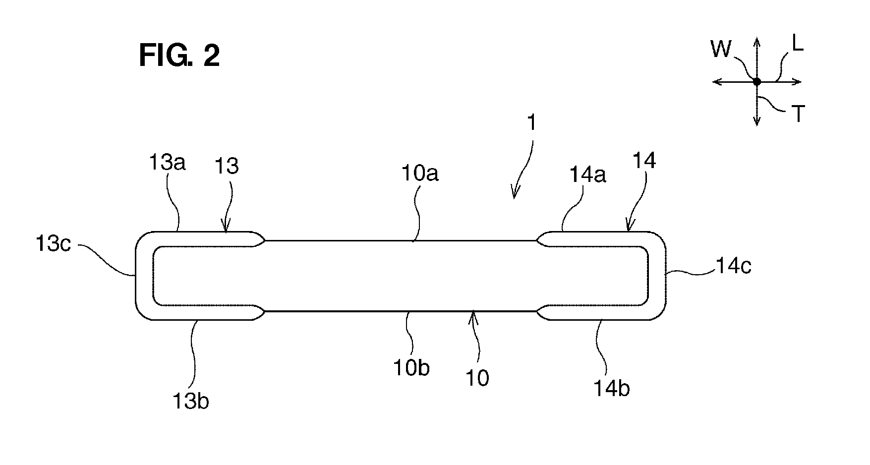
[0025]FIG. 1 is a schematic perspective view of a ceramic electronic component according to a first preferred embodiment of the present invention. FIG. 2 is a schematic side view of the ceramic electronic component according to the first preferred embodiment of the present invention. FIG. 3 is a schematic cross-sectional view taken along the line III-III in FIG. 1. FIG. 4 is a schematic diagram in which the ceramic electronic component according to the first preferred embodiment of the present invention is enlarged in part.
[0026]First, an exemplary configuration of the ceramic electronic component 1 is described ...
second preferred embodiment
[0067]FIG. 8 is a schematic perspective view of a ceramic electronic component according to a second preferred embodiment of the present invention.
[0068]The first preferred embodiment is an example in which both the first and second external electrodes 13 and 14 are disposed on each of the first and second major surfaces 10a and 10b. However, preferred embodiments of the present invention are not limited to this configuration and can be any configuration as long as at least one external electrode is disposed on the first major surface 10a.
[0069]For example, as illustrated in FIG. 8, the first and second external electrodes 13 and 14 may be disposed so as to cover the first major surface 10a and one of the first and second end surfaces 10e and 10f. That is, the first and second external electrodes 13 and 14 are not limited to particular shapes as long as the first and second external electrodes 13 and 14 include the first sections 13a and 14a, respectively, and are electrically coup...
third preferred embodiment
[0070]FIG. 9 is a schematic perspective view of a ceramic electronic component according to a third preferred embodiment of the present invention.
[0071]The first preferred embodiment is an example in which the first and second internal electrodes 11 and 12 extend to the first and second end surfaces 10e and 10f, respectively, the first and second external electrodes 13 and 14 are disposed on the first and second end surfaces 10e and 10f, respectively, and the first and second internal electrodes 11 and 12 are thus electrically coupled to the first and second external electrodes 13 and 14, respectively. However, preferred embodiments of the present invention are not limited to this configuration.
[0072]For example, as illustrated in FIG. 9, via-hole electrodes 25a and 25b may be provided, the first and second internal electrodes 11 and 12 may connect to the first and second major surfaces 10a and 10b, respectively, and the first and second internal electrodes 11 and 12 may be electric...
PUM
| Property | Measurement | Unit |
|---|---|---|
| Thickness | aaaaa | aaaaa |
Abstract
Description
Claims
Application Information