Illumination device

Inactive Publication Date: 2012-01-26
IRIS OHYAMA
View PDF4 Cites 67 Cited by
  • Summary
  • Abstract
  • Description
  • Claims
  • Application Information

AI Technical Summary

Problems solved by technology

For example, although the housing of a task light which uses an LED can be molded extremely thin in comparison with a task light which uses an incandescent lamp or a fluorescent lamp, the small thickness of the housing makes it difficult to provide controlling elements (a power supply switch, a dimmer knob, and other components) to the housing.
The kitchen illumina

Method used


Image

  • Illumination device
  • Illumination device
  • Illumination device

Examples


Embodiment Construction

[0122]

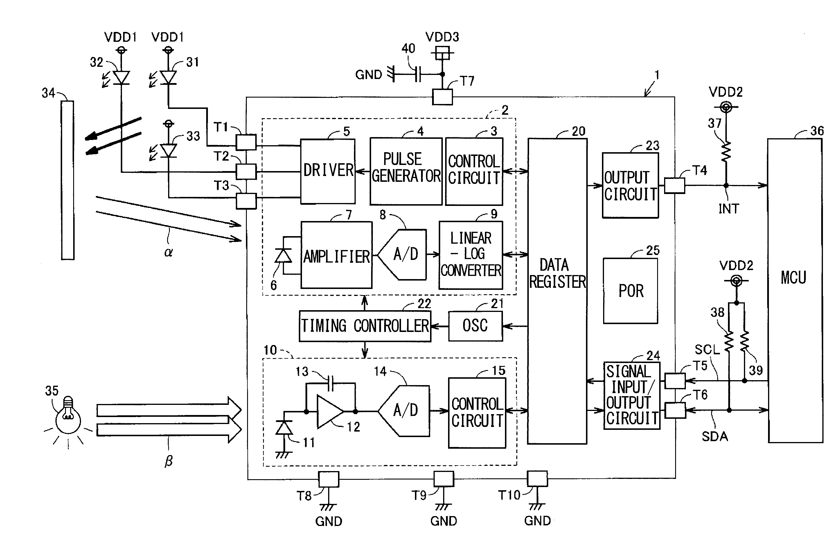
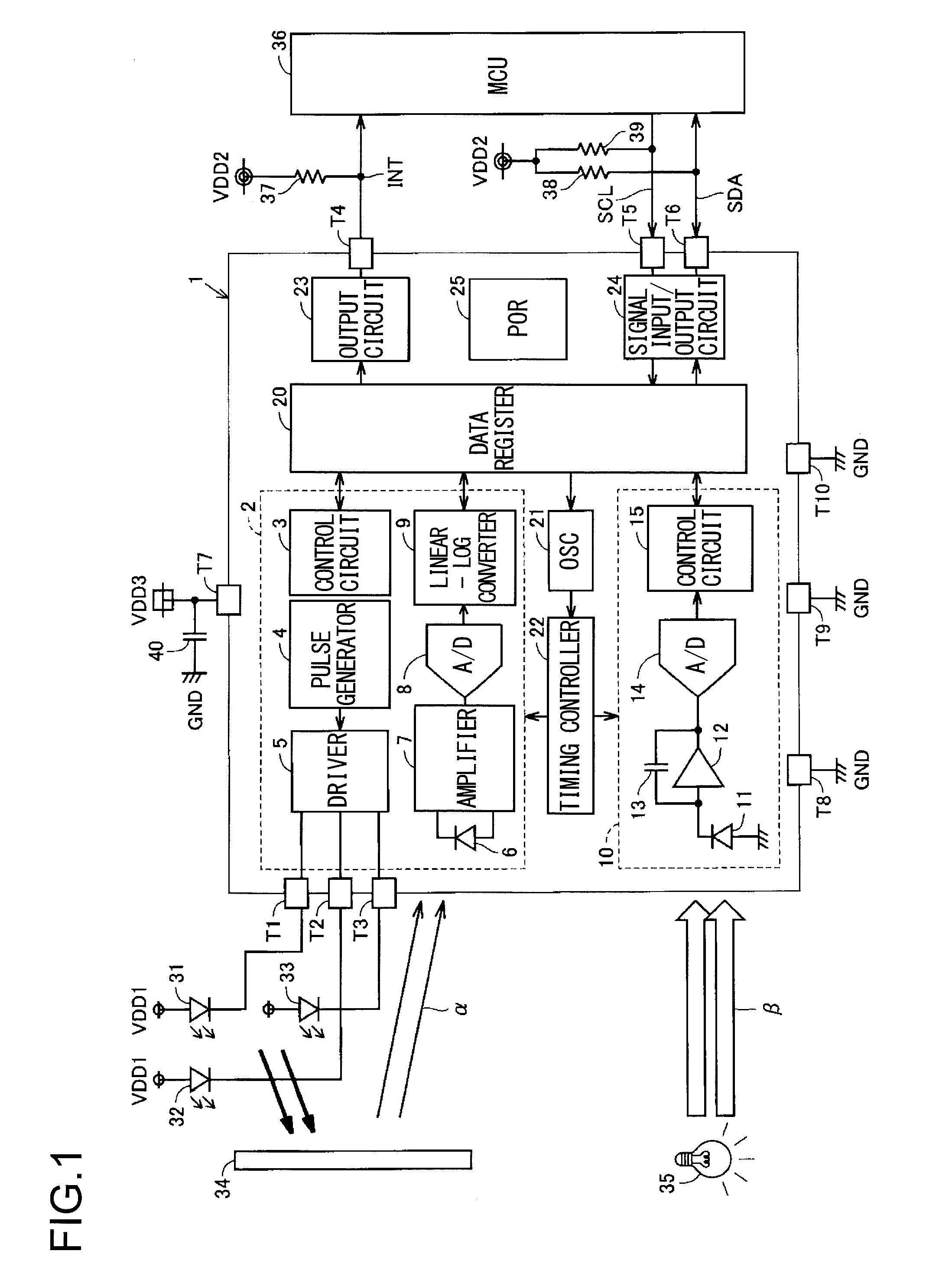
[0123]FIG. 1 is a block diagram showing the configuration of a semiconductor device. The semiconductor device 1 according to the present configuration example is provided with a proximity sensor 2, an illuminance sensor 10, a data register 20, an oscillator (OSC) 21, a timing controller 22, a signal output circuit 23, a signal input / output circuit 24, drive terminals T1 through T3, a signal output terminal T4, a clock input terminal T5, a serial data input / output terminal T6, a power supply terminal T7, ground terminals T8, T9, and a test terminal T10, as shown in FIG. 1.

[0124]The cathodes of infrared LEDs (Light Emitting Diode) 31 through 33 are connected to the drive terminals T1 through T3, respectively. The anodes of the infrared LEDs 31 through 33 each receive a power supply voltage VDD1. The proximity sensor 2 includes a control circuit 3, a pulse generator 4, a driver 5, an infrared light sensor 6, an amplifier 7, an A / D converter 8, and a linear-log converter 9. The co...


PUM


Abstract

The illumination device disclosed in the present specification has a light source, a touchless sensor for detecting proximity and movement of an object without contact, and a control unit for controlling the driving of the light source on the basis of an output of the touchless sensor.

Description

CROSS-REFERENCE TO RELATED APPLICATIONS[0001]This application is based on the following Japanese applications, the contents of which are hereby incorporated by reference.[0002](1) Japanese Patent Application No. 2010-164969 (Filing date: Jul. 22, 2010)[0003](2) Japanese Patent Application No. 2010-187077 (Filing date: Aug. 24, 2010)[0004](3) Japanese Patent Application No. 2011-099117 (Filing date: Apr. 27, 2011)BACKGROUND OF THE INVENTION[0005]1. Field of the Invention[0006]Of the various technical features disclosed in the present specification, a first technical feature relates to an illumination device provided with a dimmer function or a toning function, for example.[0007]Of the various technical features disclosed in the present specification, a second technical feature relates to an LED illumination system for illuminating a reading table in a library, for example.[0008]2. Description of Related Art[0009]<First Background Technique and Problems Thereof>[0010]Illuminatio...

Claims


Application Information

Patent Timeline
IPC IPC(8): H05B37/02
CPCG08C17/02G08C2201/91H05B33/0863Y02B20/44Y02B20/40H05B37/0227H05B45/20H05B47/115H05B47/125
Inventor IGAKI, MASARUOSAWA, HIDEHARUTSUCHIKAWA, TAKUYA
Owner IRIS OHYAMA
Why Eureka
Try Eureka