Optical waveguide device

a waveguide and optical technology, applied in the field of optical waveguide devices, can solve the problems of easy damage to thin plates, reduced product yield, and complicated optical waveguide devices, and achieve the effects of high refractive index, easy realization of high performance, and high refractive index

Active Publication Date: 2012-01-26
SUMITOMO OSAKA CEMENT CO LTD
View PDF3 Cites 3 Cited by
  • Summary
  • Abstract
  • Description
  • Claims
  • Application Information

AI Technical Summary

Benefits of technology

[0024]According to the first aspect of the invention, the optical waveguide device includes the thin plate having a thickness of 20 μm or less and at least an optical waveguide formed in the thin plate, the thin plate is bonded and fixed to a supporting substrate with an adhesive interposed therebetween, and a film having a higher refractive index (hereinafter, referred to as a ‘high refractive index film’) than the thin plate and the adhesive is provided on a surface of the thin plate bonded and fixed to the supporting substrate so as to be in contact with or close to at least a part of the optical waveguide. Accordingly, it becomes possible to configure various kinds of members, such as an optical waveguide and a diffraction grating, using the high refractive index film, and it becomes also possible to arrange various kinds of members on both surfaces of the thin plate. As a result, an optical waveguide device having multiple functions and high performance can be easily realized. In addition, since it is possible to suppress local concentration of mechanical or thermal stress in the thin plate, it is possible to prevent the thin plate from being damaged or an operating characteristic of the optical waveguide device from changing. As a result, it becomes possible to provide an optical waveguide device which is excellent in terms of productivity and has an operating characteristic that is stabilized.
[0025]According to the second aspect of the invention, since the thin plate is formed of a material having a nonlinear optical effect or an electro-optical effect, it becomes possible to provide various kinds of optical waveguide devices, such as an optical harmonic generator, a light modulator, a variable wavelength filter, or an optical switch.
[0026]According to the third aspect of the invention, since the electrode or the heater for controlling the intensity, the wave front, or the phase of light propagating through the optical waveguide is formed on the other surface of the thin plate not bonded and fixed to the supporting substrate, it becomes possible to provide various kinds of optical waveguide devices, such as an optical harmonic generator, a light modulator, a variable wavelength filter, or an optical switch.
[0027]According to the fourth aspect of the invention, since the high refractive index film is formed so as to be periodically separated in the guiding direction of the optical waveguide, the high refractive index film can function as a diffraction grating. As a result, it becomes possible to obtain an optical waveguide device, such as a wavelength filter.
[0028]According to the fifth aspect of the invention, the light detection means for detecting either the scattered light from the optical waveguide formed with the high refractive index film or the led-out light obtained by causing a part of light propagating through the optical waveguide to be led out by means of the high refractive index film and a control means for controlling a voltage or a current applied to the electrode on the basis of the amount of light detected by the light detection means are further included, and the intensity, the wave front, or the phase of light propagating through the optical waveguide is controlled. Accordingly, it becomes possible to provide a high-performance optical waveguide device capable of monitoring a light wave propagating inside the optical waveguide device and controlling a driving state of the optical waveguide device.
[0029]According to the sixth aspect of the invention, since the high refractive index film is formed in the strip line shape, the high refractive index film can be used as an optical waveguide. Thus, since the high refractive index film can be used as a bent optical waveguide or the like, it becomes possible to provide a high-performance optical waveguide device.

Problems solved by technology

As a result, the optical waveguide device itself becomes complicated.
Furthermore, if the members described above are formed on the thin plate described above, the thin plate is easily damaged due to a difference between coefficients of thermal expansion of the thin plate and each of the members or due to mechanical or thermal stress distortion caused by the complicated shape of the thin plate.
As a result, problems that yield of products decreases, unnecessary stress is applied to the thin plate and an operating characteristic of the optical waveguide device deteriorates, and the like occur.

Method used


Image

  • Optical waveguide device
  • Optical waveguide device
  • Optical waveguide device

Examples


first embodiment

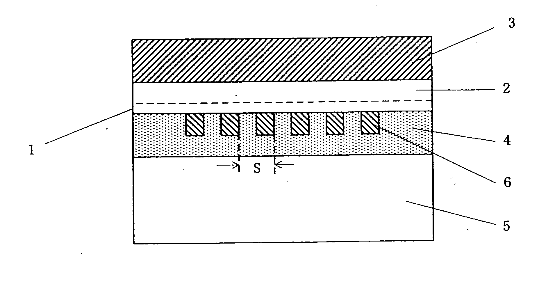
[0054]FIG. 2 is a cross-sectional view illustrating an optical waveguide device according to the invention and shows an example of the cross-sectional shape of the optical waveguide device taken along a dashed-dotted line A of FIG. 1.

[0055]High refractive index films 6 are formed on a lower surface of the thin plate 1 at a predetermined period (distance s) therebetween. Due to the shape of such high refractive index film, the high refractive index film functions as a diffraction grating with respect to the optical waveguide 2, and the optical waveguide device can operate as a wavelength filter.

[0056]A wavelength λ to be selected is determined by the relationship of λ=2 ns / m (where ‘n’ is an effective refractive index of a light wave, ‘s’ is an array period of high refractive index films, and ‘m’ is a natural number). In addition, it is possible to change the wavelength to be selected by changing the intensity of an electric field applied by the electrode 3. In this case, the optical...

second embodiment

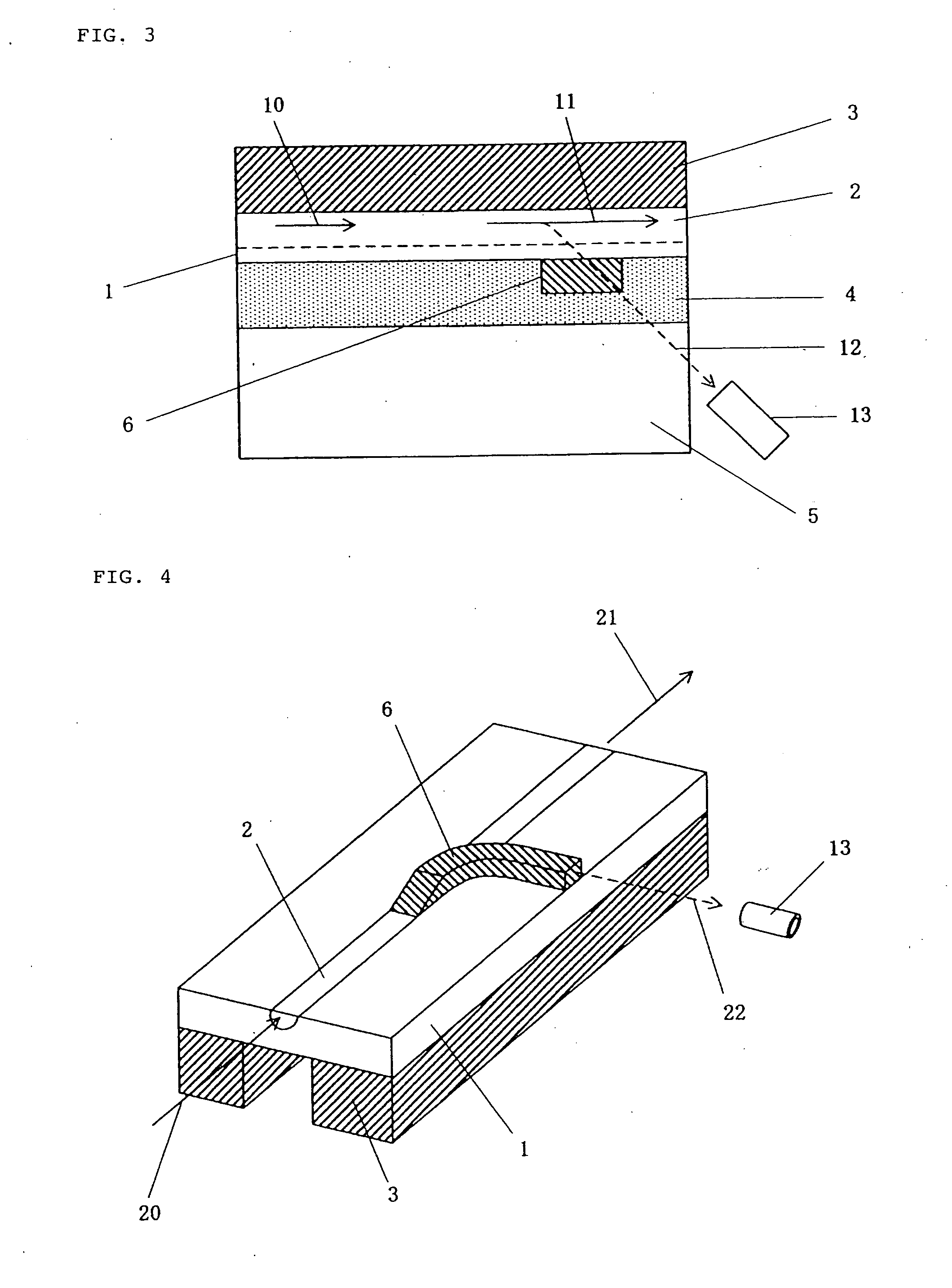
[0059]FIG. 3 is a cross-sectional view illustrating an optical waveguide device according to the invention and shows an example of the cross-sectional shape of the optical waveguide device taken along the dashed-dotted line A of FIG. 1.

[0060]The high refractive index film 6 is arranged so as to be in contact with or close to a part of the optical waveguide 2, and a part of electric waves 10 propagating through the optical waveguide 2 is led to the outside of the optical waveguide device as indicated by a dotted line 12. A part of light waves is led to the outside, but the remaining light waves 11 keep propagating through the optical waveguide. Therefore, a state of light waves propagating inside the optical waveguide device can be easily monitored and determined by detecting the led-out light 12 with a photodetector 13.

[0061]The shape of the high refractive index film 6 shown in FIG. 3 is not limited to only the thing of a rectangular parallelepiped. For example, even if the shape i...

third embodiment

[0063]FIG. 4 illustrates an optical waveguide device according to the invention.

[0064]In FIG. 4, the supporting substrate 5 and the bonding layer 4 included in the optical waveguide device are omitted in order to clearly show the appearance of the high refractive index film formed on a surface of the thin plate 1. In addition, the bonding layer and the supporting substrate are arranged at an upper side of the thin plate 1 shown in FIG. 4.

[0065]The optical waveguide 2 is formed on a surface of the thin plate 1, and the control electrode 3 is formed on the other surface of the thin plate 1. The high refractive index film 6 that is in contact with the optical waveguide 2 and has a strip line shape is formed in a shape shown in FIG. 4. The high refractive index film 6 becomes thick along the optical waveguide 2 and is bent in the middle so as to be separated from the optical waveguide 2.

[0066]By providing the high refractive index film 6, a part of light waves 20 incident on the optical...


PUM

PropertyMeasurementUnit
thicknessaaaaaaaaaa
thicknessaaaaaaaaaa
refractive indexaaaaaaaaaa

Abstract

An optical waveguide device having multiple functions or high performance, to improve the productivity of products, and to provide an optical waveguide device capable of suppressing deterioration of an operating characteristic of the optical waveguide device, including a thin plate 1 having a thickness of 20 μm or less, and at least an optical waveguide 2 formed in the thin plate. The thin plate is bonded and fixed to a supporting substrate 5 with an adhesive 4 interposed therebetween, and a film having a higher refractive index than the thin plate is provided on a surface of the thin plate bonded and fixed to the supporting substrate so as to be in contact with a part of the optical waveguide.

Description

TECHNICAL FIELD[0001]This application is a divisional of application Ser. No. 12 / 225,783 filed Dec. 12, 2008, which was a §371 of PCT / JP2007 / 054233 filed Mar. 6, 2007, claiming priority from Japan Pat. App. No. 2006-092293 filed Mar. 29, 2006, all of which are incorporated herein by reference. The present invention relates to an optical waveguide device, and more particularly, to an optical waveguide device which uses a thin plate having a thickness of 20 μm or less and has at least an optical waveguide formed in the thin plate.BACKGROUND ART[0002]In an optical communication field or an optical measurement field, an optical waveguide device in which an optical waveguide or modulation electrodes are formed on a substrate having an electro-optical effect or the like has been often used in the related art.[0003]In particular, since the amount of transmitted information tends to increase with the development of multimedia, it is necessary to widen a band of a light modulation frequency....

Claims


Application Information

Patent Timeline
Patent Type & Authority Applications(United States)
IPC IPC(8): G02F1/01G02B6/12
CPCG02B6/125G02F1/035G02B6/4204
Inventor ICHIKAWA, JUNICHIRO
Owner SUMITOMO OSAKA CEMENT CO LTD
Why Eureka
Try Eureka