Semiconductor structure having a contact-level air gap within the interlayer dielectrics above a semiconductor device and a method of forming the semiconductor structure using a self-assembly approach
a technology of interlayer dielectrics and semiconductor devices, applied in the direction of semiconductor devices, semiconductor/solid-state device details, electrical apparatus, etc., can solve the problems of affecting device performance, increasing device power consumption, and reducing device speed
- Summary
- Abstract
- Description
- Claims
- Application Information
AI Technical Summary
Benefits of technology
Problems solved by technology
Method used
Image

Examples
Embodiment Construction
[0028]The embodiments of the invention and the various features and advantageous details thereof are explained more fully with reference to the non-limiting embodiments that are illustrated in the accompanying drawings and detailed in the following description.
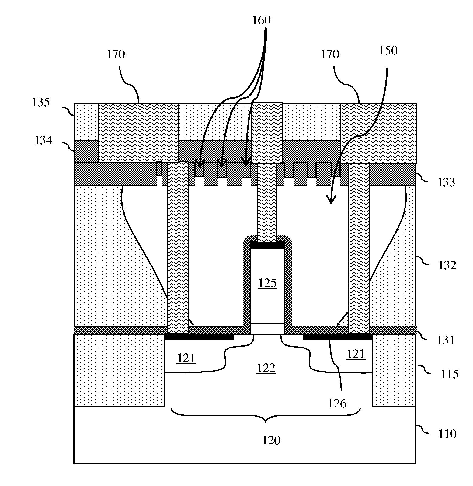
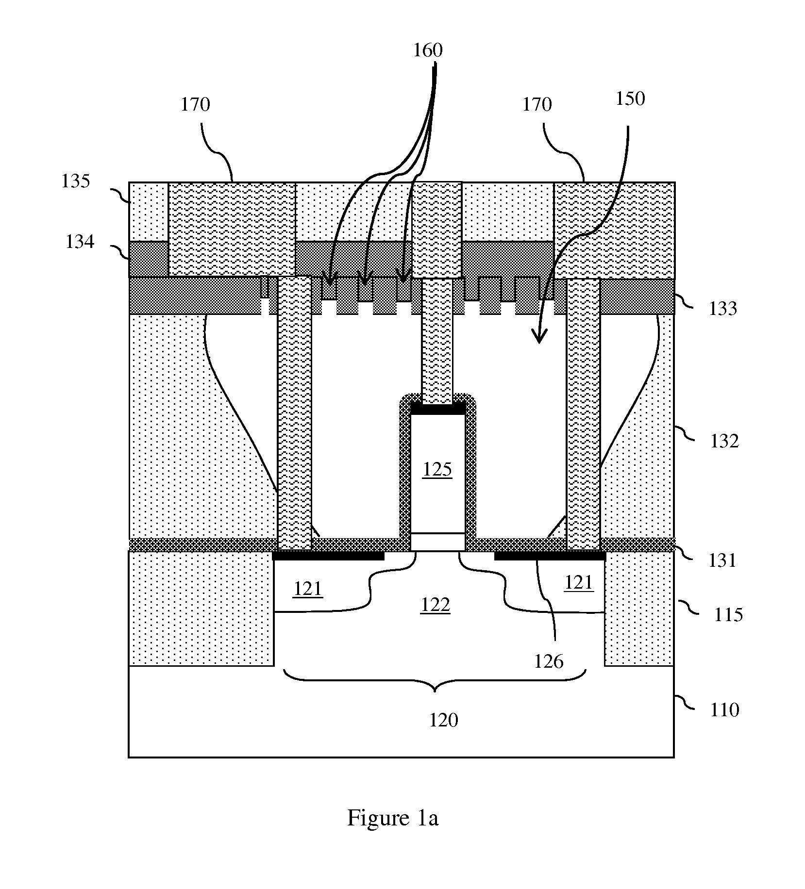
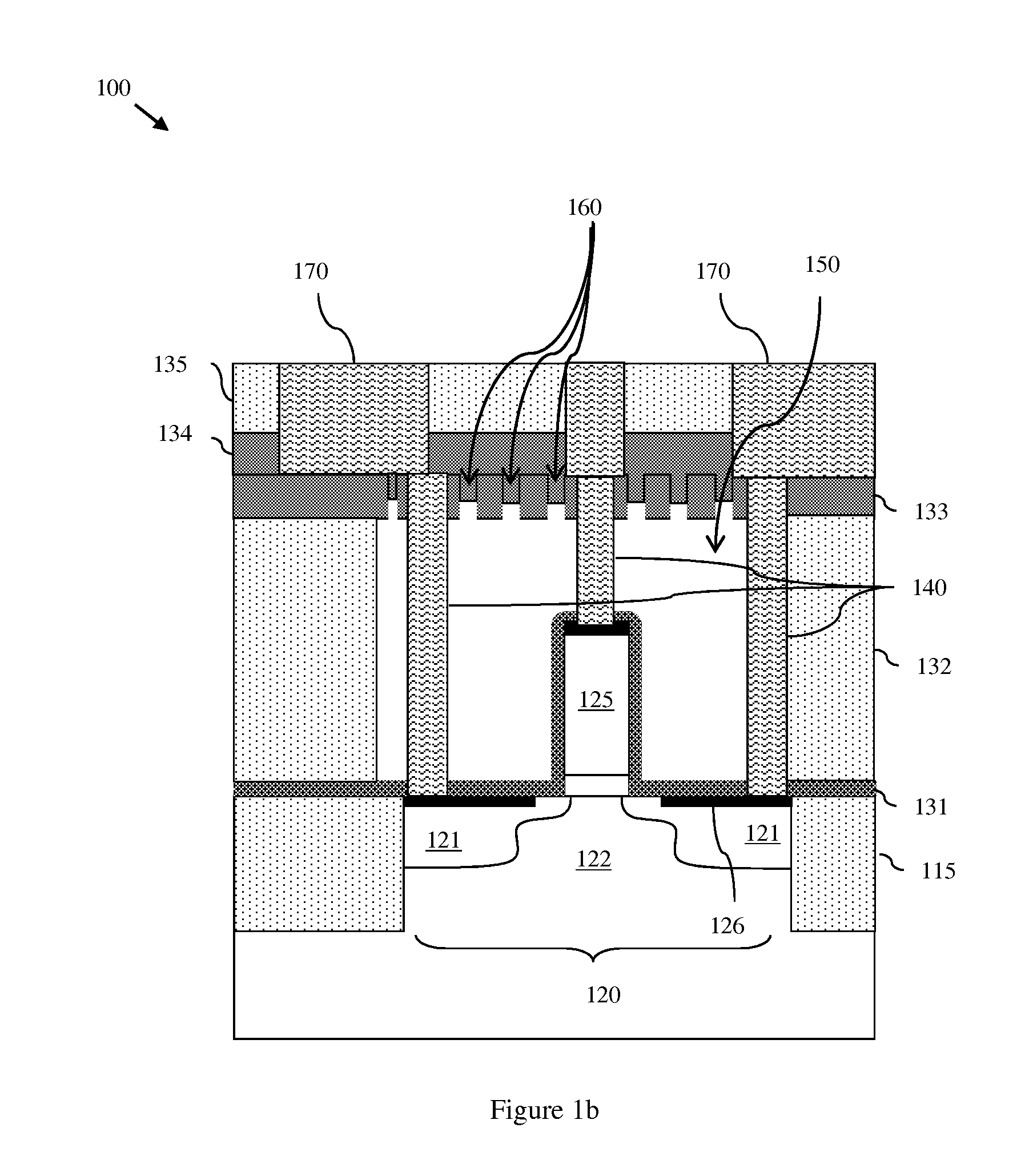
[0029]As discussed above, contact-level interlayer dielectrics and sidewall spacers are typically formed of a combination of dielectric materials (e.g., silicon dioxide (SiO2) with a dielectric constant of 3.9, silicon nitride (Si3N4) with a dielectric constant of 7.5, etc.), thereby resulting in devices that exhibit relatively high parasitic capacitances (e.g., contact-to-contact capacitance, contact-to-diffusion region capacitance, gate-to-contact capacitance, gate-to-diffusion region capacitance, etc.). Such parasitic capacitances can increase device power consumption and can impact device performance (e.g., decrease device speed).
[0030]Various techniques can be used to minimize these parasitic capacitances. For example, Si...
PUM
 Abstract
Description
Claims
Application Information