Magnetic sensor and magnetic detection apparatus

Active Publication Date: 2012-02-16
TDK CORPARATION
View PDF9 Cites 13 Cited by
  • Summary
  • Abstract
  • Description
  • Claims
  • Application Information

AI Technical Summary

Benefits of technology

[0022]The present invention successively provides the magnetic sensor capable of

Problems solved by technology

However, the conventional magnetic sensors using the spin accumulation failed to provi

Method used


Image

  • Magnetic sensor and magnetic detection apparatus
  • Magnetic sensor and magnetic detection apparatus
  • Magnetic sensor and magnetic detection apparatus

Examples


Example

[0062]FIG. 7 is a cross-sectional view showing modification example 2 of the magnetic sensor. The magnetic sensor 4 shown in FIG. 7 is different in the arrangement of the channel layer, ferromagnetic layer, metal layer, insulating films, first reference electrode, second reference electrode, and magnetic shield layer from the magnetic sensor 1. The present example shows a configuration wherein the magnetic sensor 4 detects the external magnetic field in the Y-axis direction. The magnetic sensor 4 is provided with a channel layer 11a composed of a semiconductor, a ferromagnetic layer 12a, a metal layer 13a, insulating films 21a, 22a, 24a, 24b, a first reference electrode 31a, a second reference electrode 32a, and magnetic shield layers S1a, S3, S4. The insulating film (first insulating film in this example) 21a and the metal layer 13a are arranged opposite to each other with the channel layer 11a in between. The ferromagnetic layer 12a is provided on the insulating film 21a opposed t...

Example

EXAMPLE 1

[0069]First, as shown in FIG. 8(a), an SOI substrate 40 consisting of a substrate SB, an insulating film 23, and a channel layer 11 was prepared. A silicon substrate was used as the substrate SB, a silicon oxide layer 200 nm thick as the insulating film 23, and a silicon layer 5 nm thick as the channel layer 11. Then the SOI substrate 40 was cleaned to remove extraneous matter, organic matter, and native oxide IN in FIG. 8(a)) from the surface of the channel layer 11, thereby obtaining the SOT substrate 40 shown in FIG. 8(b). A cleaning solution used herein was a diluted HF solution. Subsequently, as shown in FIG. 8(c), an insulating film 21, a ferromagnetic layer 12, and a protecting layer 15 were deposited in this order on the channel layer 11 by the MBE process. A magnesium oxide film was used as the insulating film 21, an iron layer as the ferromagnetic layer 12, and a titanium layer as the protecting layer 15. Thereafter, a first resist R1 was formed on the protecting...

Example

[0073]In Examples 2 to 5, the magnetic sensors were manufactured in the same procedure as in Example 1 except for change in the thickness of the silicon layer being the channel layer 11. In Example 2 the thickness of the silicon layer was 10 nm; in Example 3 the thickness of the silicon layer 25 nm; in Example 4 the thickness of the silicon layer 50 nm; in Example 5 the thickness of the silicon layer 100 nm.

[0074](Evaluation Results)

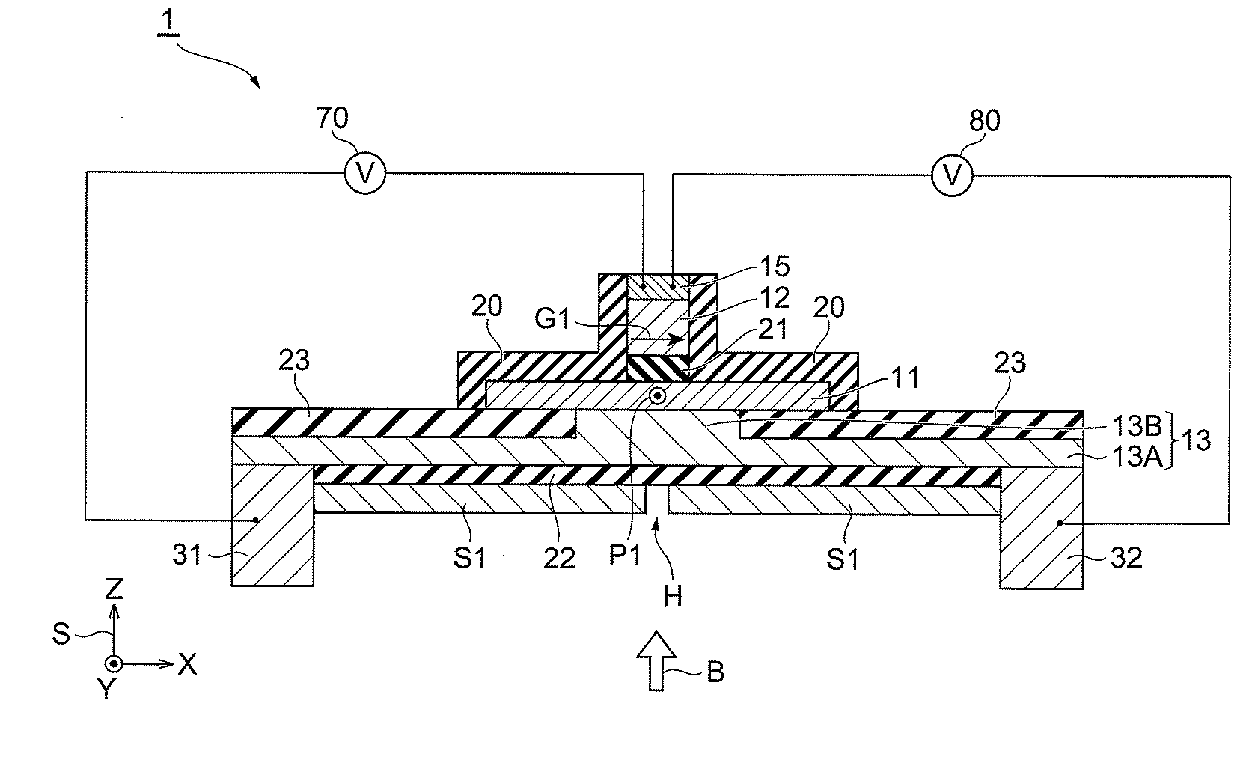
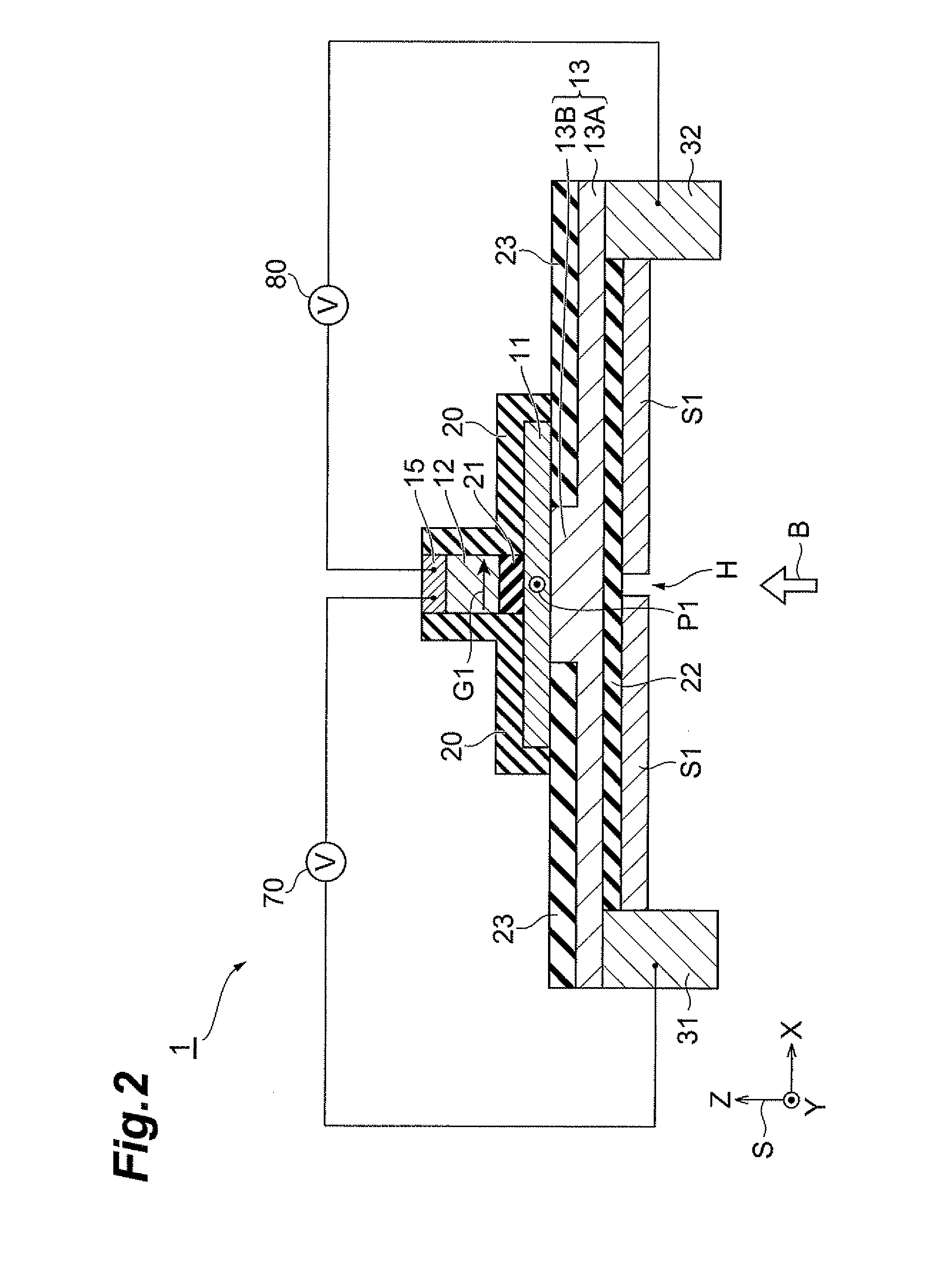
[0075]In each of the magnetic sensors manufactured in Examples 1 to 5, the magnetization direction G1 of the ferromagnetic layer 12 (X-axis direction in FIG. 2) was fixed so as to be nonparallel to the magnetic field direction of the external magnetic field B (Z-axis direction in FIG. 2). The ferromagnetic layer 12 and the first reference electrode 31 were connected to a current source 70. By adjusting the current source 70, a negative voltage was applied to the ferromagnetic layer 12 while a positive voltage was applied to the first reference electrode ...


PUM


Abstract

A magnetic sensor is provided with a channel of a semiconductor, a first insulating film and a metal body arranged opposite to each other with the channel in between, a ferromagnet provided on the first insulating film, a first reference electrode connected to the metal body, a second reference electrode connected to the metal body, a magnetic shield covering a portion opposed to the ferromagnet in the channel, and a second insulating film provided between the channel and the magnetic shield. The magnetic shield has a through hole extending toward the portion opposed to the ferromagnet in the channel.

Description

BACKGROUND OF THE INVENTION[0001]1. Field of the Invention[0002]The present invention relates to a magnetic sensor and magnetic detection apparatus using spins.[0003]2. Related Background Art[0004]It is recently known that spins injected from a ferromagnet into a nonmagnetic body are accumulated there and the spins are attenuated by an external magnetic field, as described in Non-patent Literature 1 (X. Lou et al., “Electrical Detection of Spin Accumulation at a Ferromagnet-Semiconductor Interface,” PHYSICAL REVIEW LETTERS, The American Physical Society, May 5, 2006, 96, 176603-1 to 176603-4). It is also known that spins are accumulated in a semiconductor. The semiconductor for accumulation of spins is GaAs, for example, as employed in Non-patent Literature 2 (M. Tran et al., “Enhancement of the Spin Accumulation at the Interface between a Spin-Polarized Tunnel Junction and a Semiconductor,” PHYSICAL REVIEW LETTERS, The American Physical Society, Jan. 23, 2009, 102, 036601-1 to 0366...

Claims


Application Information

Patent Timeline
IPC IPC(8): G01R33/02
CPCG01R33/1284G11C11/16
Inventor SASAKI, TOMOYUKIOIKAWA, TOHRU
Owner TDK CORPARATION
Why Eureka
Try Eureka