

Semiconductor device having both IGBT area and diode area
a technology of igbt and diode, which is applied in the direction of semiconductor devices, basic electric elements, electrical apparatus, etc., can solve the problems of increasing diode loss, increasing diode loss, and increasing diode loss, so as to improve the recovery characteristics of diode elements and reduce the properties of igbt
- Summary
- Abstract
- Description
- Claims
- Application Information
AI Technical Summary
Benefits of technology
Problems solved by technology
Method used
Image

Examples
first embodiment
[0039]A first embodiment of the present invention will be described with reference to the drawings. A semiconductor device described in the present embodiment is used as, for example, a power switching element for a power supply circuit such as an inverter or a DC / DC converter.
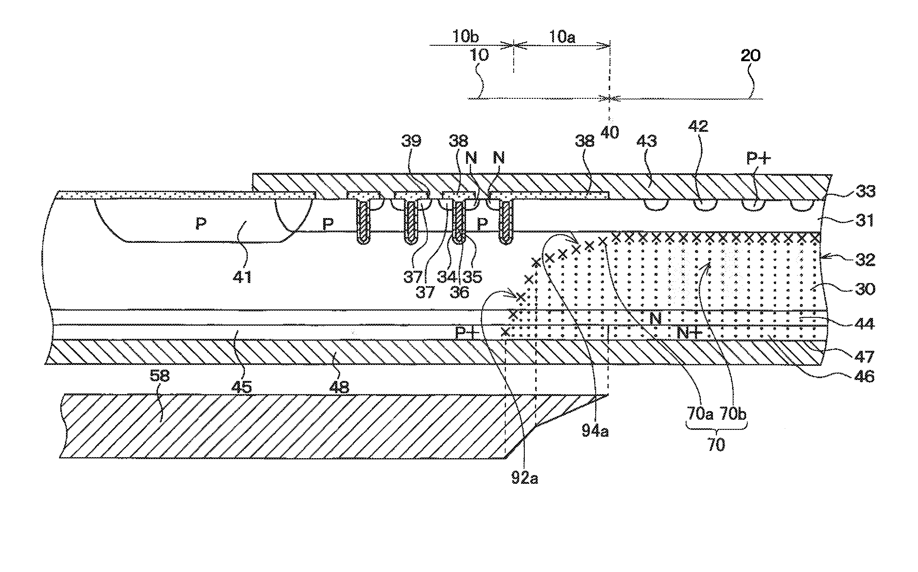
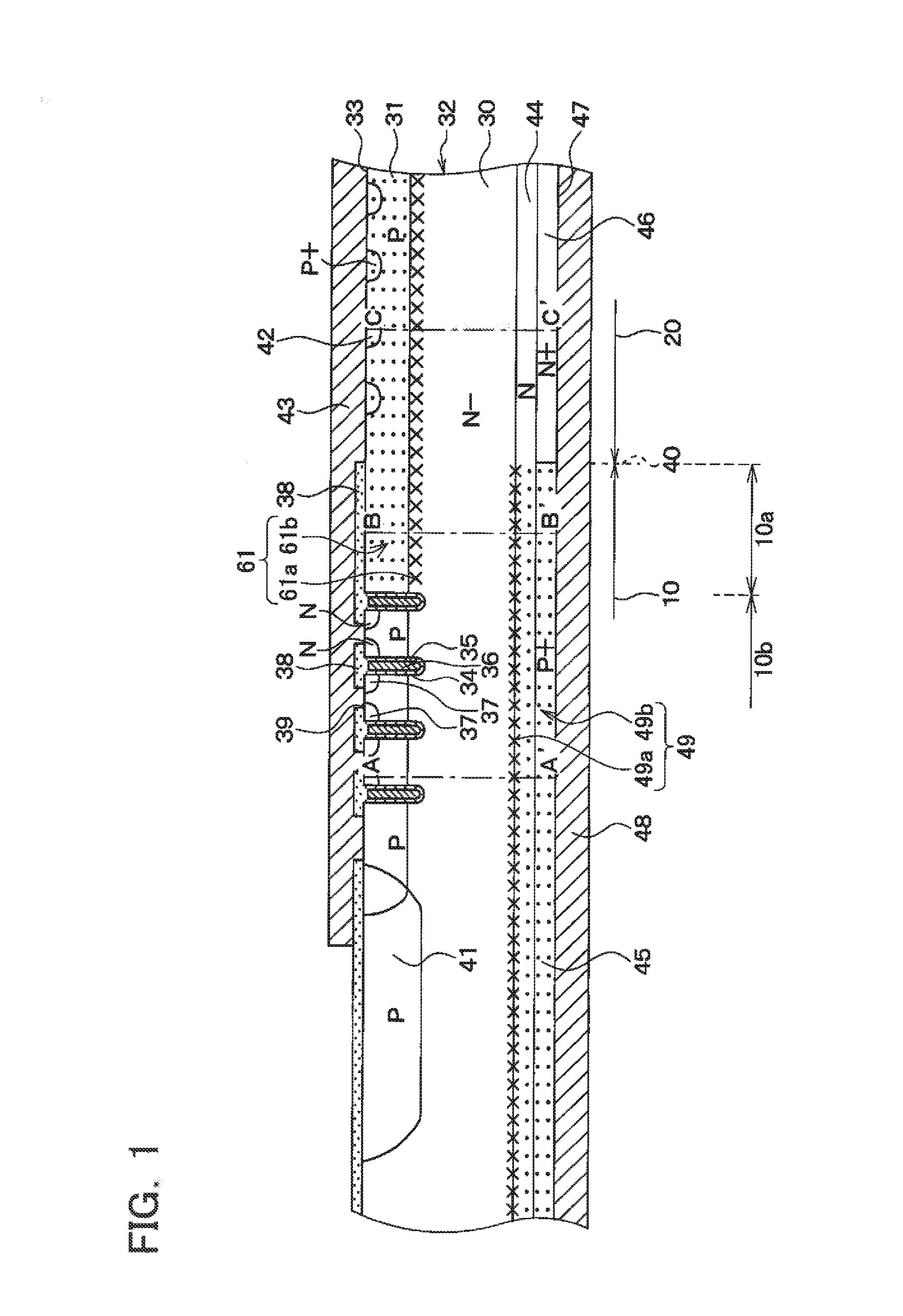
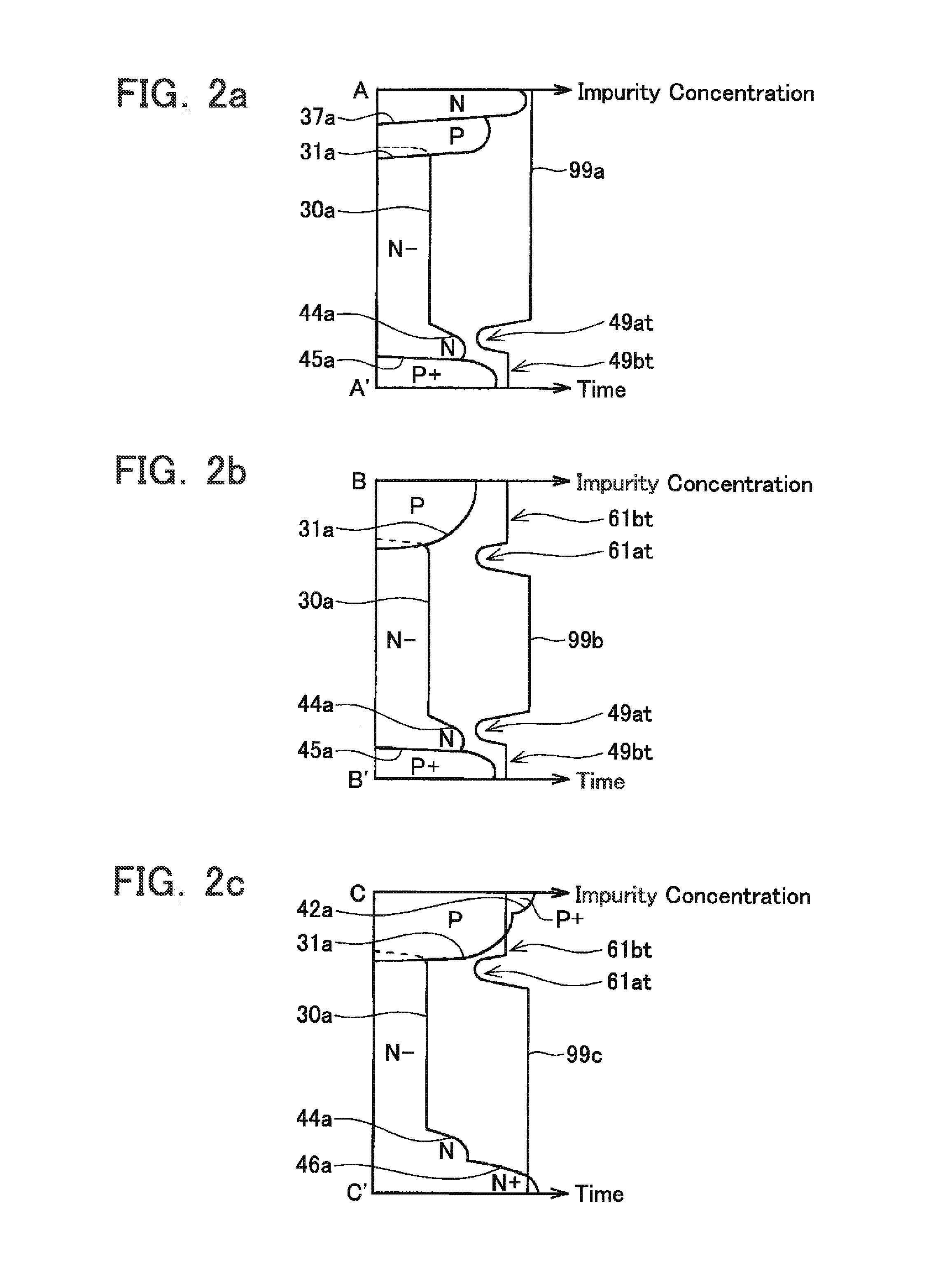
[0040]FIG. 1 is a cross-sectional view of a semiconductor device according to the present embodiment. As shown in the drawing, the semiconductor device includes an IGBT area 10 and a diode area 20. The IGBT area 10 and the diode area 20 are formed on a same semiconductor substrate 32. The IGBT area 10 is formed in an area adjacent to the diode area 20.
[0041]An N− silicon wafer is used as the unprocessed semiconductor substrate 32. As shown in FIG. 1, at the IGBT area 10 and the diode area 20, P-type impurities are implanted from a surface 33 of the semiconductor substrate 32 and subjected to heat treatment to form a P-type base layer 31. At the IGBT area 10 and the diode area 20, N-type impurities are implante...
second embodiment
[0068]In the present embodiment, portions that differ from the first embodiment will be described. FIG. 4 is a cross-sectional view of a semiconductor device according to the present embodiment. The cross-sectional view in FIG. 4 also shows an He ion mask 51 for forming a lifetime shortening region 49 and a He ion mask 50 for forming a lifetime shortening region 62.
[0069]As shown in FIG. 4, in the present embodiment, the lifetime shortening region 49 is formed by exposing an IGBT area 10 (both a complete sub-area 10b and an incomplete sub-area 10a) among a rear surface 47 of the semiconductor substrate 32 to He ions using the mask 51. In addition, the lifetime shortening region 62 is formed by exposing the incomplete sub-area 10a and a diode area 20 among the rear surface 47 of the semiconductor substrate 32 to He ions using the mask 50.
[0070]When exposing the IGBT area 10 to He ions using the mask 51, He ions are implanted with an energy that causes the He ions to penetrate into th...
third embodiment
[0077]In the present embodiment, portions that differ from the first embodiment will be described. FIG. 6 is a cross-sectional view of a semiconductor device according to the present embodiment which also shows a mask 52 for forming lifetime shortening regions 49, 63, and 72.
[0078]As shown in FIG. 6, a rear surface of a He ion mask 52 according to the present embodiment is inclined at a certain angle at an incomplete sub-area 10a. In other words, the mask 52 is thick at a complete sub-area 10b and becomes thinner toward a diode area 20 at the incomplete sub-area 10a.
[0079]When a semiconductor substrate 32 is exposed to He ions by arranging the He ion mask 52 on the side of a rear surface 47 of the semiconductor substrate 32, a penetration distance of the He ions is short at a thick portion of the mask 52. The penetration distance of the He ions becomes longer as the mask 52 becomes thinner, and penetration is deepest at an area not covered by the mask 52.
[0080]In FIG. 6, a lifetime...
PUM
 Abstract
Description
Claims
Application Information