

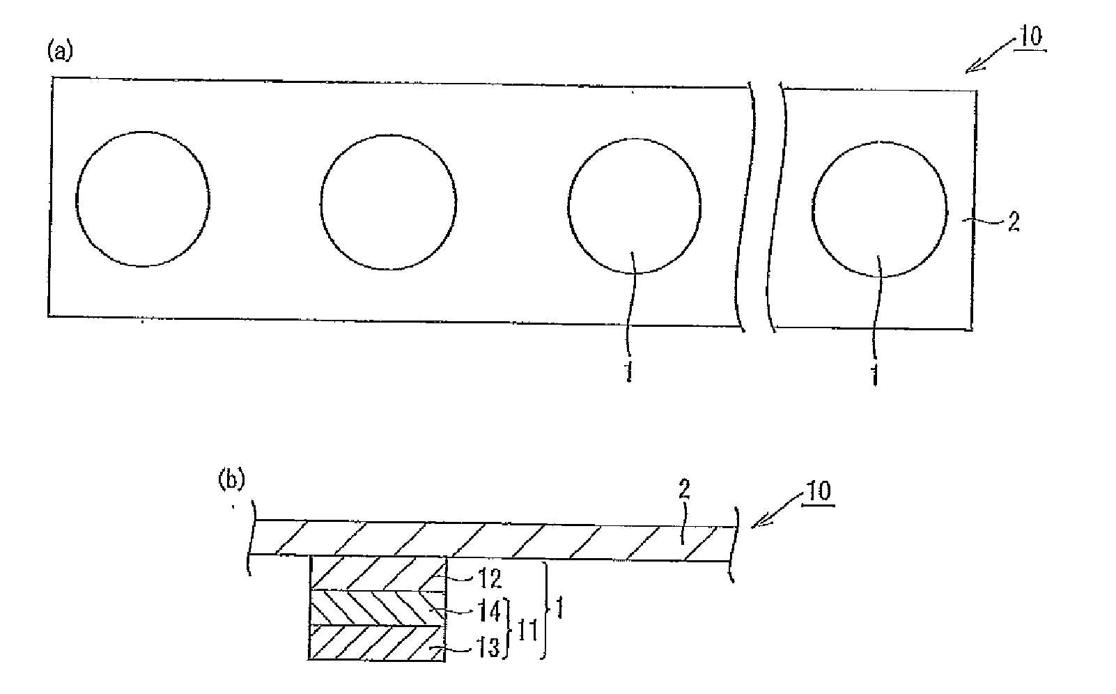
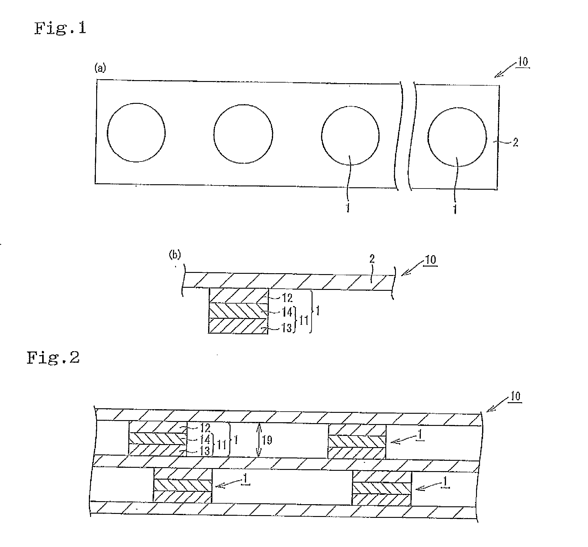
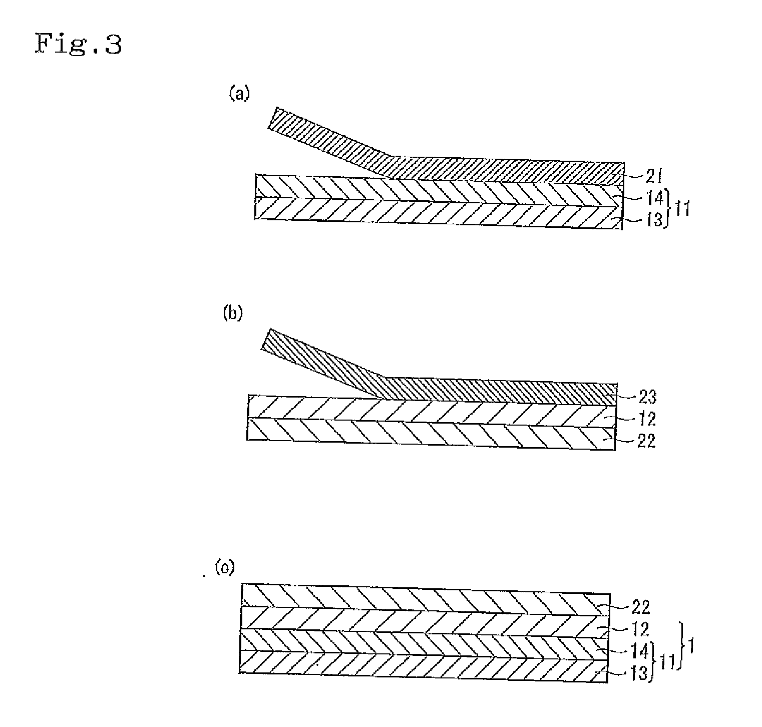
Film for semiconductor device, and semiconductor device
a technology for semiconductor devices and films, applied in the direction of film/foil adhesives, transportation and packaging, synthetic resin layered products, etc., can solve the problems of reducing the yield of semiconductor devices manufactured, loss of adhesive film flatness, etc., and achieve the smallest shrinkage, the effect of preventing the film lifting phenomenon of the cover film, and the largest shrinkage degr
- Summary
- Abstract
- Description
- Claims
- Application Information
AI Technical Summary
Benefits of technology
Problems solved by technology
Method used
Image

Examples
example 1
Production of Pressure-Sensitive Adhesive Layer of Dicing Film
[0129]An acrylic polymer A having a weight average molecular weight of 800,000 was obtained by placing 80 parts of 2-ethylhexylacrylate (2EHA), 20 parts of 2-hydroxyethylacrylate (HEA), 0.2 parts of benzoyl peroxide, and 60 parts of toluene into a reactor having a cooling tube, a nitrogen introducing tube, a thermometer, and a stirrer and performing a polymerization treatment at 61° C. in a nitrogen gas stream for 6 hours. The molar ratio of 2EHA to HEA was 100 mol to 20 mol. The measurement of the weight average molecular weight was performed as described above. The weight average molecular weight was measured by GPC (Gel Permeation Chromatography) and calculated by polystyrene conversion.
[0130]An acrylic polymer A′ was obtained by adding 10 parts (80 mol % relative to HEA) of 2-methacryloyloxyethyl isocyanate (referred to as “MOI” in the following) into the acrylic polymer A and performing an addition reaction treatment...
example 2
Production of Dicing Film
[0142]The same dicing film as in Example 1 was used as the dicing film according to this example.
[0143]In methylethylketone, 1 part of an isocyanate crosslinking agent (trade name: Coronate HX manufactured by Nippon Polyurethane Industry Co., Ltd.), 400 parts of an o-cresol novolac-type epoxy resin (trade name: EOCN-1027 manufactured by Nippon Kayaku Co., Ltd.), 400 parts of a phenol resin (trade name: Milex XLC-LL manufactured by Mitsui Chemicals, Inc.), and 100 parts of spherical silica (trade name: SO-25R manufactured by Admatechs Co., Ltd., average particle size 0.5 μm) as an inorganic filler to 100 parts of an acrylic ester polymer (trade name: Paracron W-197CM manufactured by Negami Chemical Industries Co., Ltd., Tg: 18° C., weight average molecular weight: 400,000) having ethylacrylate-methylmethacrylate as a main component were dissolved, and the concentration was adjusted to be 20.0% by weight.
[0144]The film for a semiconductor device according to E...
PUM
| Property | Measurement | Unit |
|---|---|---|
| temperature | aaaaa | aaaaa |
| glass transition temperature | aaaaa | aaaaa |
| tensile storage modulus Eb | aaaaa | aaaaa |
Abstract
Description
Claims
Application Information