Methods and apparatus for detecting molecular interactions using fet arrays

a technology of molecular interactions and arrays, applied in biochemistry apparatus and processes, instruments, electrochemical variables of materials, etc., can solve the problems of unpredictability of transmission gate operation, or preclude operation entirely, so as to improve the density of the passivation layer, enhance chemical vapor deposition, and reduce porosity

Active Publication Date: 2012-03-15
LIFE TECH CORP
View PDF4 Cites 37 Cited by
  • Summary
  • Abstract
  • Description
  • Claims
  • Application Information

AI Technical Summary

Benefits of technology

[0075]In various aspects, the chemFET arrays may be fabricated using conventional CMOS (or biCMOS or other suitable) processing technologies, and are particularly configured to facilitate the rapid acquisition of data from the entire array (scanning all of the pixels to obtain corresponding pixel output signals).
[0078]The invention has specifically improved upon the ISFET array design of Milgrew et al. discussed above in connection with FIGS. 1-7, as well as other conventional ISFET array designs, so as to significantly reduce pixel size, and thereby increase the number of pixels of a chemFET array for a given semiconductor die size (i.e., increase pixel density). In various embodiments, this increase in pixel density is accomplished while at the same time increasing the signal-to-noise ratio (SNR) of output signals corresponding to monitored biological and chemical processes, and the speed with which such output signals may be read from the array. In particular, it has been recognized and appreciated that by relaxing requirements for chemFET linearity and focusing on a more limited measurement output signal range (e.g., output signals corresponding to a pH range of from approximately 7 to 9 or smaller, rather than 1 to 14, as well as output signals that do not necessarily relate significantly to pH), individual pixel complexity and size may be significantly reduced, thereby facilitating the realization of very large scale dense chemFET arrays. It has also been recognized and appreciated that alternative less complex approaches to pixel selection in an chemFET array (e.g., alternatives to the row and column decoder approach employed in the design of Milgrew et al. as shown in FIG. 7, whose complexity scales with array size), as well as various data processing techniques involving ISFET response modeling and data extrapolation based on such modeling, facilitate rapid acquisition of data from significantly large and dense arrays.
[0093]Another embodiment is directed to a method for processing an array of CMOS-fabricated sensors. Each sensor comprises a chemFET having a chemically-sensitive passivation layer of silicon nitride and / or silicon oxynitride deposited via plasma enhanced chemical vapor deposition (PECVD). The method comprises depositing at least one additional passivation material on the chemically-sensitive passivation layer so as to reduce a porosity and / or increase a density of the passivation layer.

Problems solved by technology

In particular, because the body and source of the p-channel ISFET are electrically coupled together, implementing the p-channel MOSFET S11P in the same n-well as the p-channel ISFET 50 would lead to unpredictable operation of the transmission gate, or preclude operation entirely.

Method used


Image

  • Methods and apparatus for detecting molecular interactions using fet arrays
  • Methods and apparatus for detecting molecular interactions using fet arrays
  • Methods and apparatus for detecting molecular interactions using fet arrays

Examples


Embodiment Construction

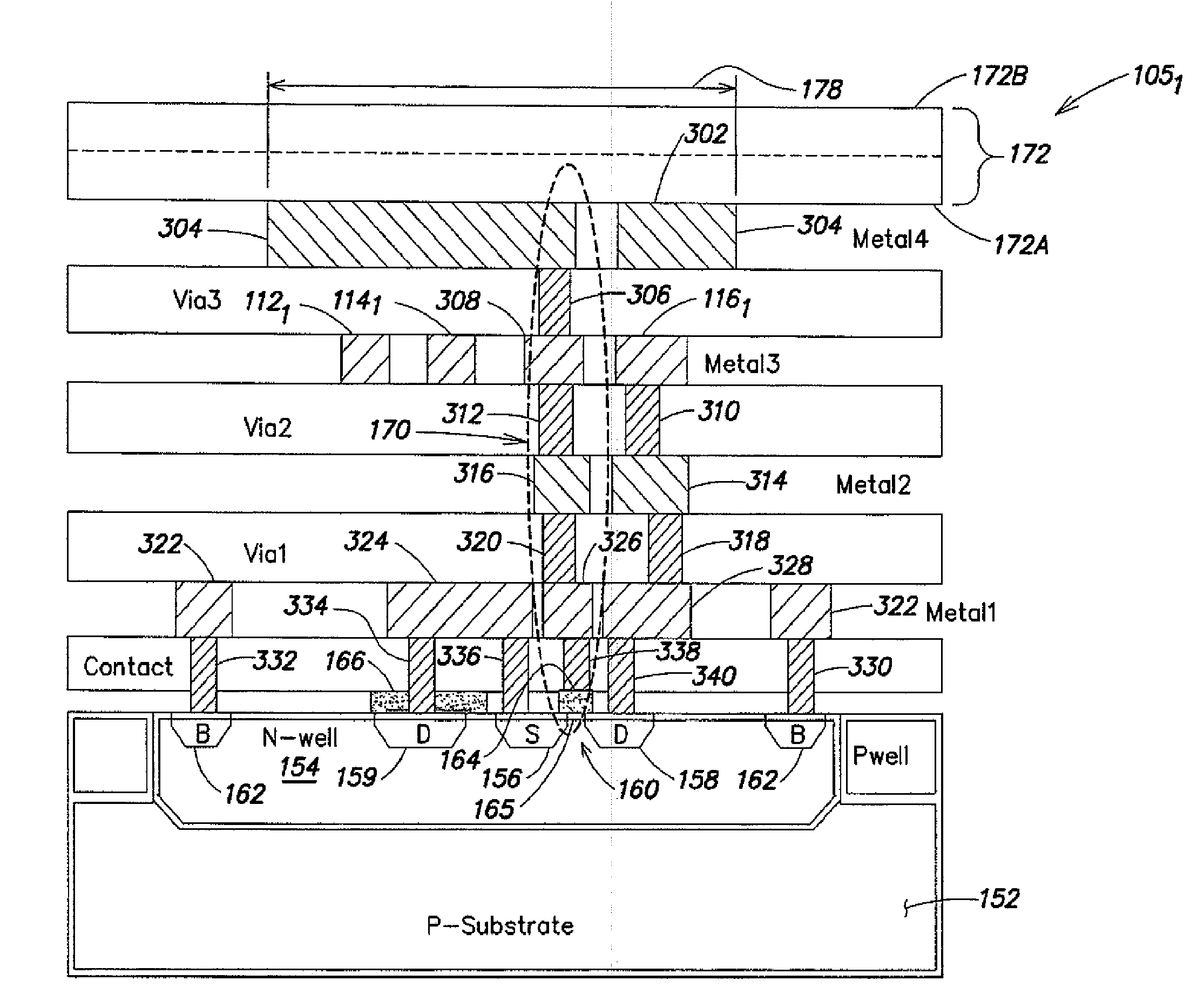
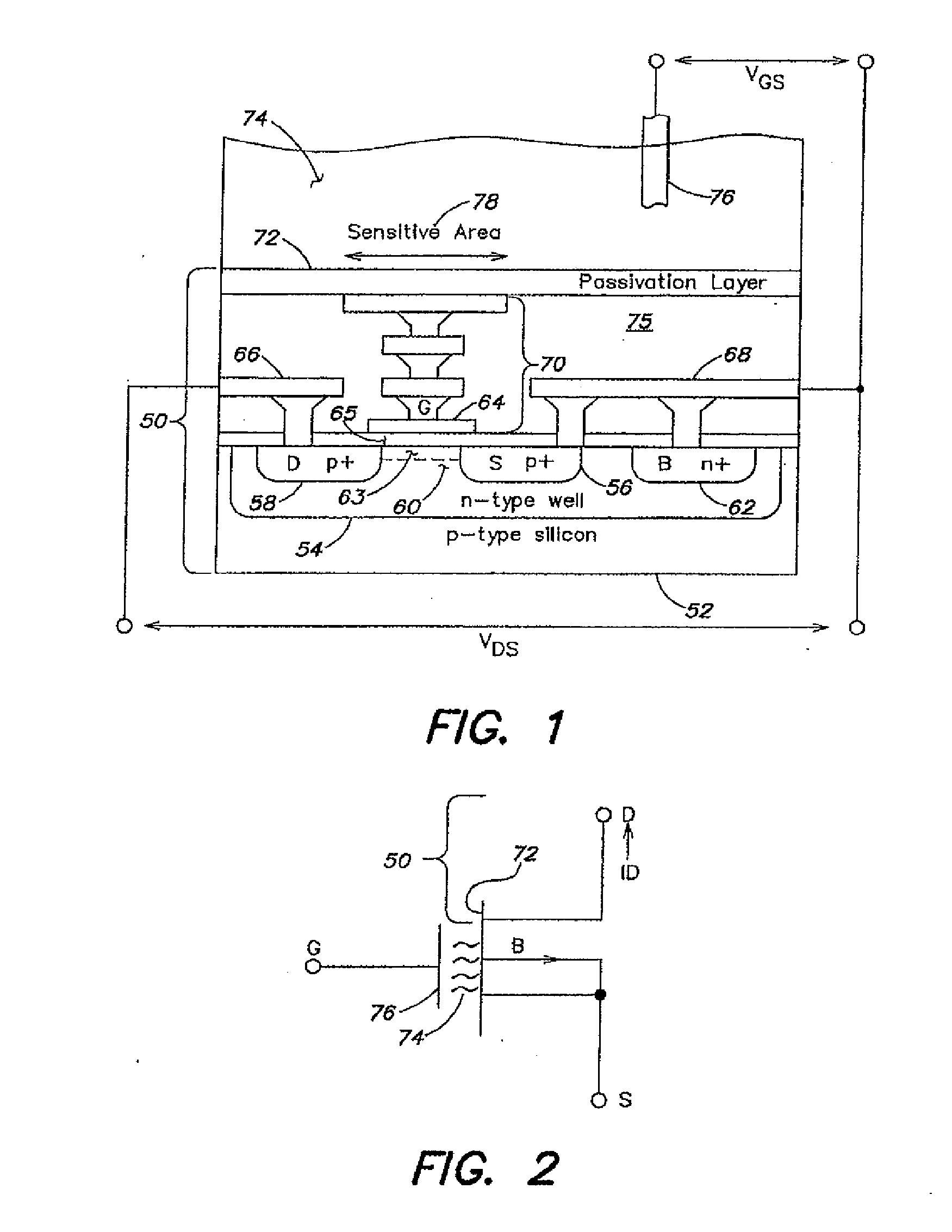
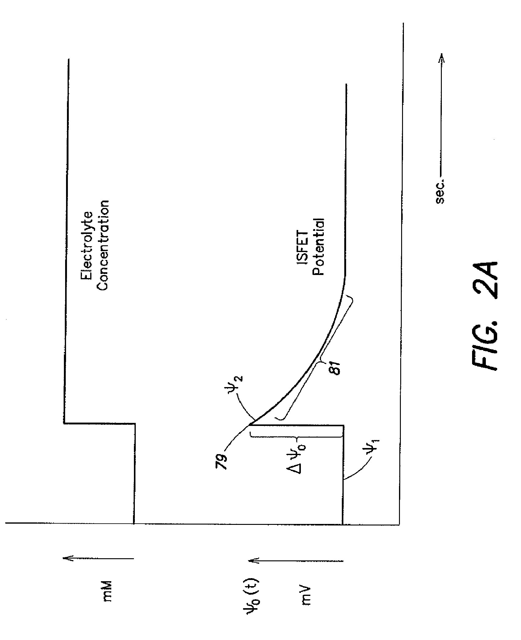
[0161]Following below are more detailed descriptions of various concepts related to, and embodiments of, inventive methods and apparatus relating to large scale chemFET arrays for detection and / or measurement or analytes. It should be appreciated that various concepts introduced above and discussed in greater detail below may be implemented in any of numerous ways, as the disclosed concepts are not limited to any particular manner of implementation. Examples of specific implementations and applications are provided primarily for illustrative purposes.

[0162]Various inventive embodiments according to the present disclosure are directed at least in part to a semiconductor-based / microfluidic hybrid system that combines the power of microelectronics with the biocompatibility of a microfluidic system. In some examples below, the microelectronics portion of the hybrid system is implemented in CMOS technology for purposes of illustration. It should be appreciated, however, that the disclosu...


PUM

PropertyMeasurementUnit
parasitic capacitanceaaaaaaaaaa
tapered shapeaaaaaaaaaa
dielectricaaaaaaaaaa

Abstract

Methods and apparatuses relating to large scale FET arrays for analyte detection and measurement are provided. ChemFET (e.g., ISFET) arrays may be fabricated using conventional CMOS processing techniques based on improved FET pixel and array designs that increase measurement sensitivity and accuracy, and at the same time facilitate significantly small pixel sizes and dense arrays. Improved array control techniques provide for rapid data acquisition from large and dense arrays. Such arrays may be employed to detect a presence and / or concentration changes of various analyte types in a wide variety of chemical and / or biological processes.

Description

RELATED APPLICATIONS[0001]This application claims priority to U.S. provisional application 61 / 133,204 filed Jun. 26, 2008 and claims priority to and is a continuation-in-part of U.S. non-provisional application Ser. No. 12 / 002,291 filed Dec. 14, 2007, the entire contents of both of which are incorporated by reference.FIELD OF THE DISCLOSURE[0002]The present disclosure is directed generally to inventive methods and apparatus relating to detection and measurement of one or more analytes.BACKGROUND OF THE INVENTION[0003]Electronic devices and components have found numerous applications in chemistry and biology (more generally, “life sciences”), especially for detection and measurement of various chemical and biological reactions and identification, detection and measurement of various compounds. One such electronic device is referred to as an ion-sensitive field effect transistor, often denoted in the relevant literature as ISFET (or pHFET). ISFETs conventionally have been explored, pr...

Claims


Application Information

Patent Timeline
Patent Type & Authority Applications(United States)
IPC IPC(8): H01L29/788H01L21/336
CPCC12Q1/6825C12Q1/6869H01L29/78H01L2924/01006G01N27/4145C12Q1/6874G01N33/54373G01N33/6818G01N27/4148G01N27/26H01L29/788
Inventor ROTHBERG, JONATHAN M.HINZ, WOLFGANG
Owner LIFE TECH CORP
Why Eureka
Try Eureka