

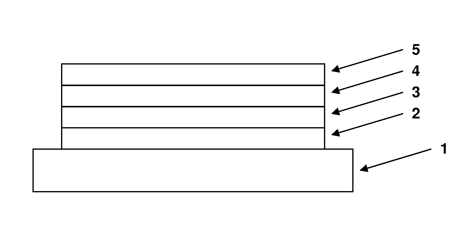
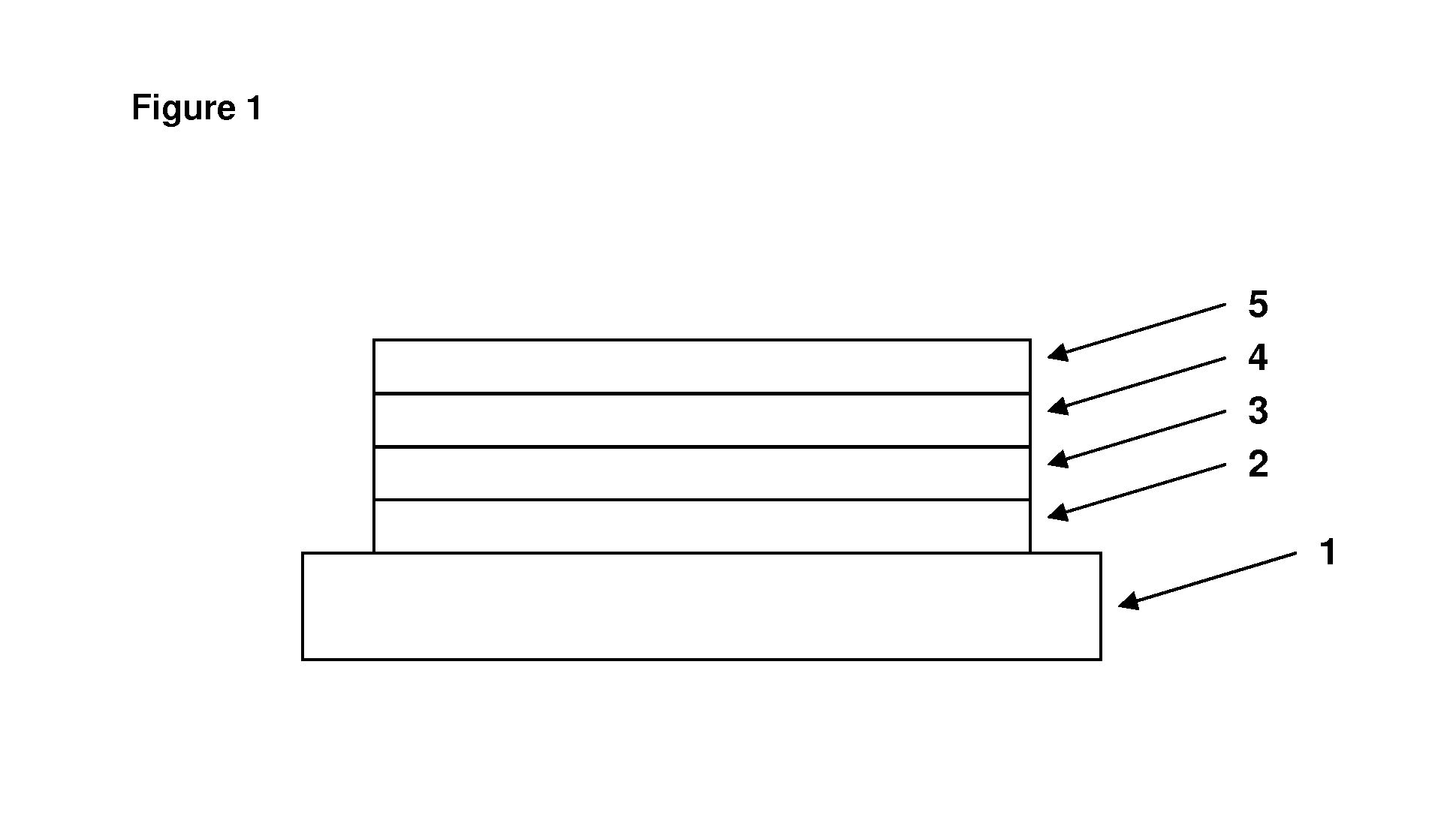
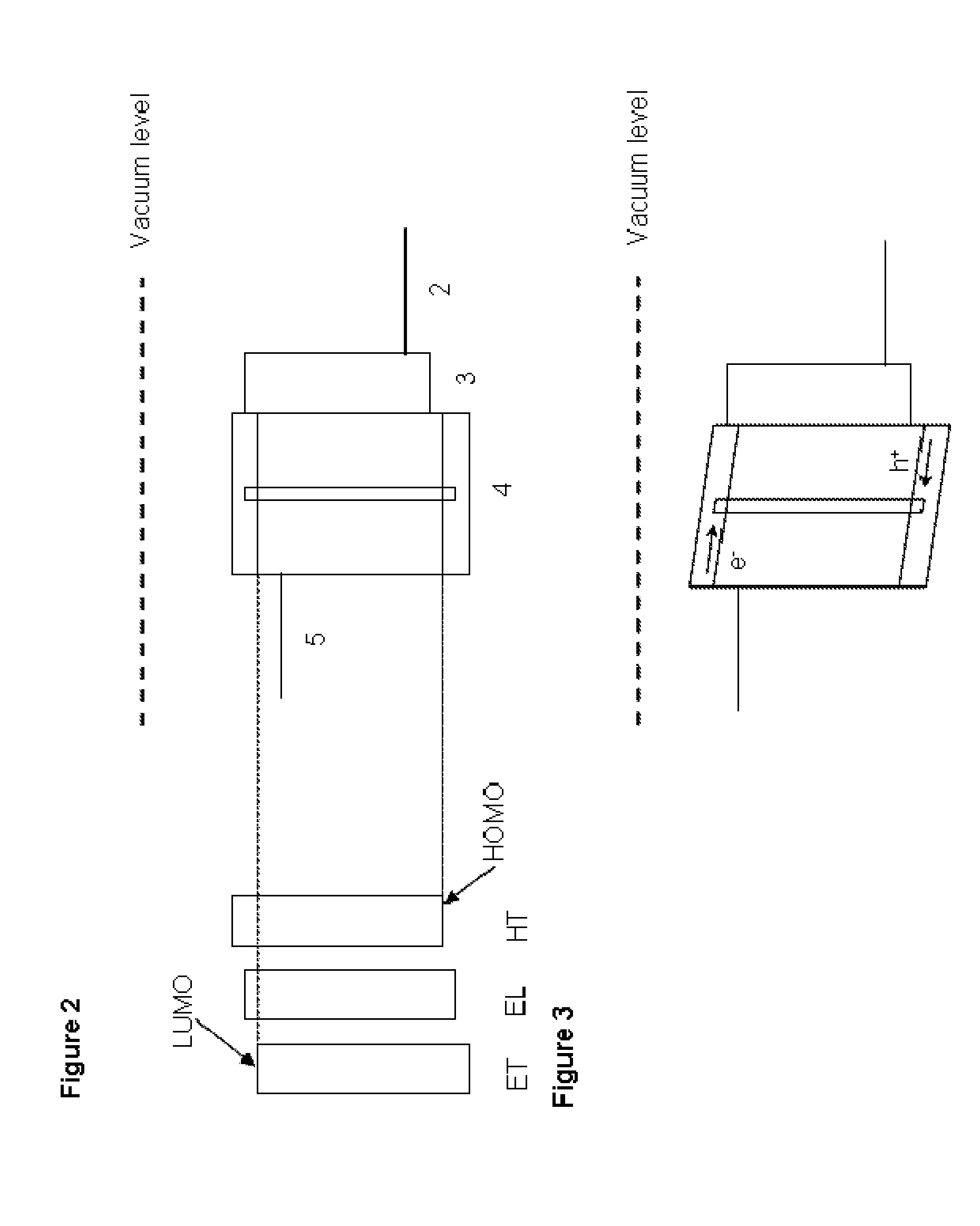
Organic Electroluminescent Device and Method of Fabrication
a technology of electroluminescent devices and materials, applied in the direction of discharge tubes/lamp details, discharge tubes luminescent screens, coatings, etc., can solve problems such as poor device performan
- Summary
- Abstract
- Description
- Claims
- Application Information
AI Technical Summary
Benefits of technology
Problems solved by technology
Method used
Image

Examples
example 1
[0122]Onto a layer of glass provided with indium tin oxide (ITO) was deposited a layer of hole injection material available from Plextronics, Inc. as Plexcore®. A 20 nm thick hole transporting electroluminescent layer was formed by depositing from solution a mixture of a polymer comprising a fluorene repeat unit and an arylamine repeat unit, and an electron trapping phosphorescent material. A 70 nm thick electroluminescent electron transporting layer was formed by depositing from solution a white-emitting polymer comprising fluorene repeat units, green and blue fluorescent emitting repeat units and a phosphorescent red emitting end-capping unit as described in GB 0801227.0. A cathode was formed by depositing a layer of sodium fluoride to a thickness of 5 nm and a capping layer of aluminium.
[0123]In Example 1, the orange-red emission from the electron trapping electroluminescent material combines with the white emission from the electron transporting layer to provide an improved whit...
PUM
 Abstract
Description
Claims
Application Information