
Nonlinear Approach to Scaling Circuit Behaviors for Electronic Design Automation

a technology of electronic design automation and behavior, applied in the field of scaling circuit behavior, can solve the problems of increasing the cost of design errors, increasing the complexity of integrated circuits, increasing the cost of development, etc., and achieve the effect of avoiding recalculation for each scaling task

Active Publication Date: 2012-03-29
SYNOPSYS INC
View PDF1 Cites 0 Cited by
  • Summary
  • Abstract
  • Description
  • Claims
  • Application Information

AI Technical Summary

Benefits of technology

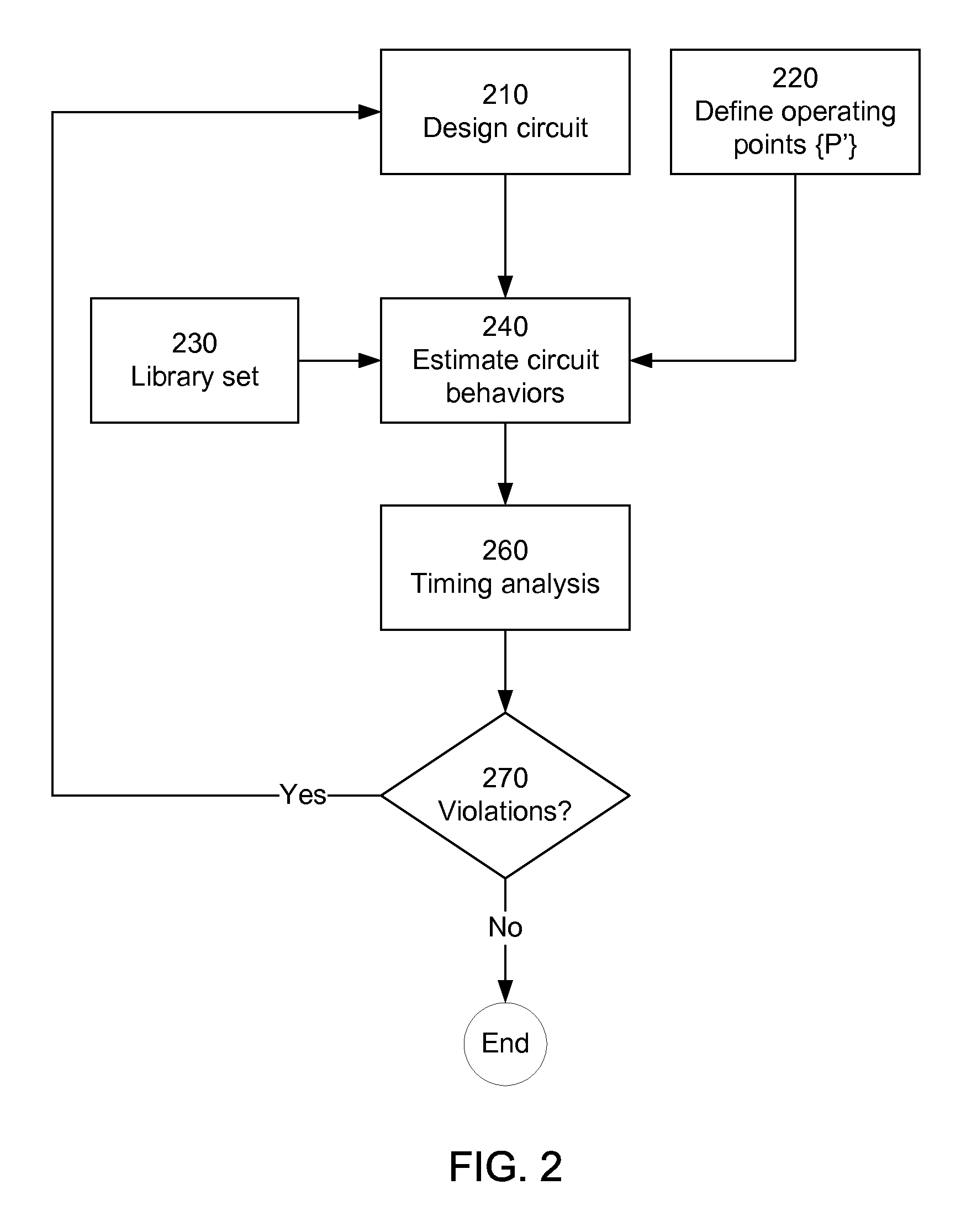
[0009]In one aspect, circuit behaviors are scaled to different operating conditions by using a generalized nonlinear model. Nonlinear transforms are applied to the operating conditions and / or to the circuit behaviors contained in the library set. The transformed quantities have a more linear relationship between them. Parameters for the linear relationship are estimated based on the data in the library set. These parameters and nonlinear transforms can then be used to scale circuit behaviors to operating points not contained in the library set. In one approach, the parameters are calculated a priori and then accessed for each scaling task, thus avoiding recalculation for each scaling task.

Problems solved by technology

As technology progresses, integrated circuits are becoming larger and more complex.
They are also becoming more expensive to develop.
As a result, the cost of a design error is also increasing, which puts more emphasis on checking the designs before they are fabricated in order to reduce the risk of a design error.
However, the increasing size and complexity of integrated circuits, coupled with the increasing stringency of timing requirements, means that it has become necessary to use sophisticated tools to assist in this task.
Even with current technology, automated timing analysis can take a long time.
In addition, overly optimistic results will miss possible design errors and overly pessimistic results will impose unnecessary constraints on the chip design.
However, derating factors are fairly simplistic.
They are a fudge factor of sorts which can be sufficient for older process technologies but may not be sufficient as technology progresses, for example in the case of deep submicron processes.
For more complex analysis, derating factors typically do not provide sufficiently accurate results.
They also have difficulty handling scaling across many operating conditions simultaneously.

Method used


Image

  • Nonlinear Approach to Scaling Circuit Behaviors for Electronic Design Automation
  • Nonlinear Approach to Scaling Circuit Behaviors for Electronic Design Automation
  • Nonlinear Approach to Scaling Circuit Behaviors for Electronic Design Automation

Examples


Embodiment Construction

[0016]A preferred embodiment of the present invention is now described with reference to the figures where like reference numbers indicate identical or functionally similar elements. Aspects of the invention will be illustrated using static timing analysis (STA) as an example, but the invention is not limited to STA.

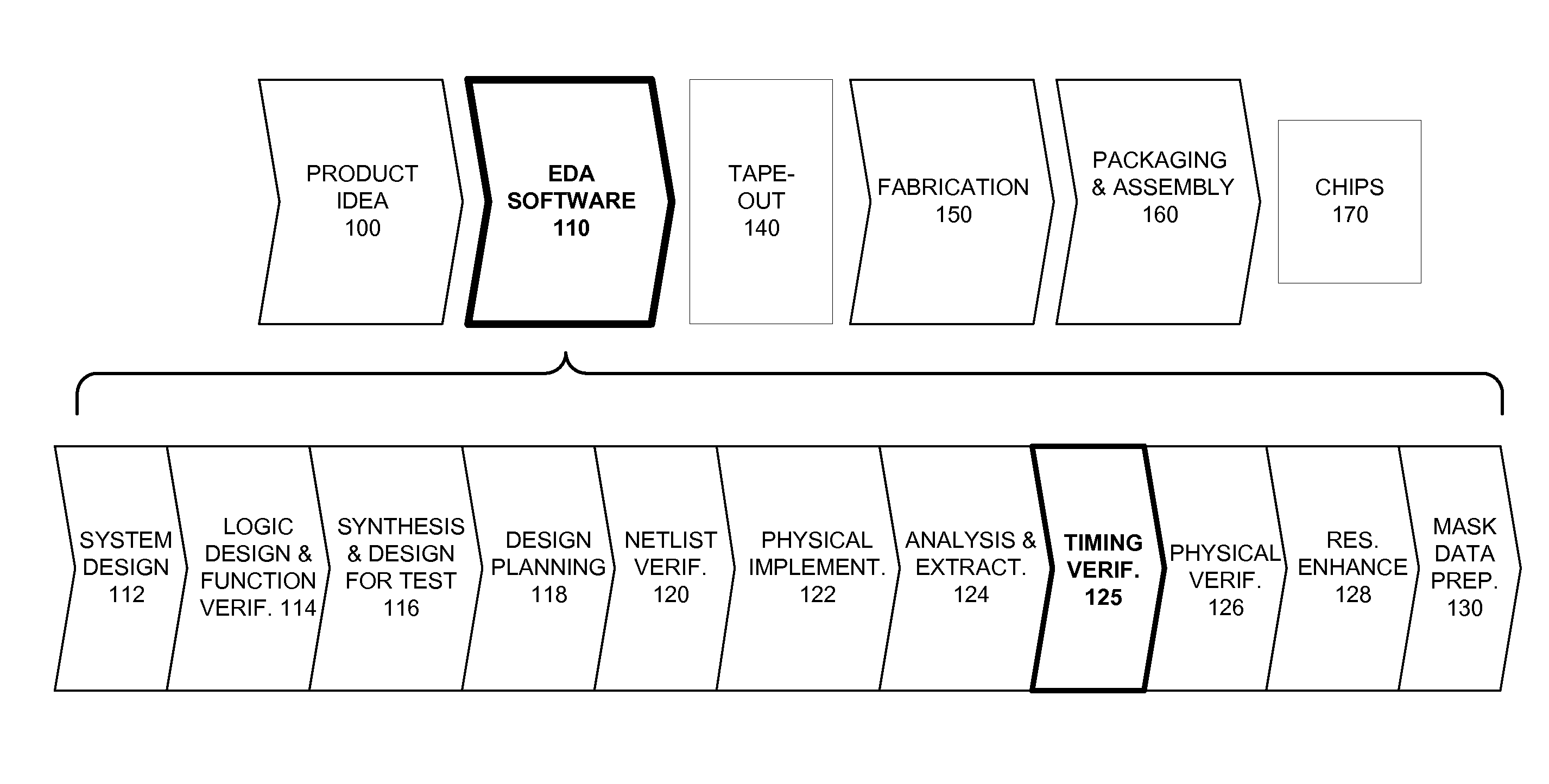
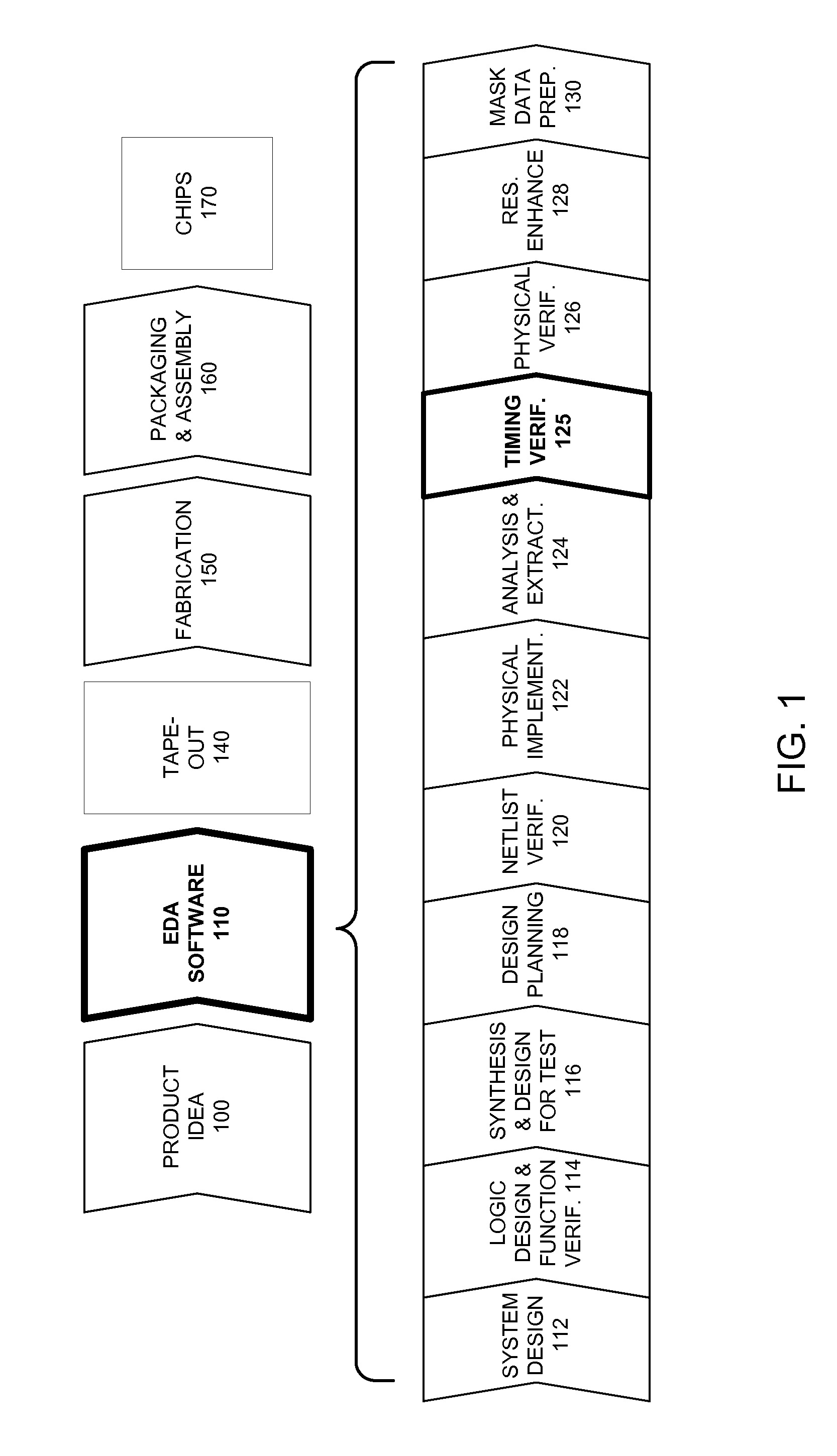
[0017]FIG. 1 illustrates the various steps in the design and fabrication of an integrated circuit in accordance with an embodiment of the present invention. The process starts with a product idea 100. Next, the product idea is realized by an integrated circuit, the design of which is accomplished using electronic design automation (EDA) software 110. Once the design is finalized, it is taped-out 140. After tape-out, the process goes through fabrication 150, and packaging and assembly 160. The process eventually culminates with the production of physical integrated circuits 170.

[0018]The EDA software design step 110, in turn, includes a number of phases. In this example, ...


PUM


Abstract

Circuit behaviors are scaled to different operating conditions by using a generalized nonlinear model. Nonlinear transforms are applied to the operating conditions and / or to the circuit behaviors contained in a library set. The transformed quantities have a more linear relationship between them. Parameters for the linear relationship are estimated based on the data and operating conditions in the library set. These parameters and nonlinear transforms can then be used to scale circuit behaviors to operating points not contained in the library set.

Description

CROSS-REFERENCE TO RELATED APPLICATION(S)[0001]This application claims priority under 35 U.S.C. §119(e) to U.S. Provisional Patent Application Ser. No. 61 / 385,870, “Nonlinear Approach To Scaling Circuit Behaviors For Electronic Design Automation,” filed Sep. 23, 2010. The subject matter of all of the foregoing is incorporated herein by reference in its entirety.FIELD OF THE INVENTION[0002]The present invention is related to scaling circuit behaviors as part of the electronic design automation (EDA) process. In a common scenario, it relates to using cell libraries that describe the circuit behavior under certain conditions, in order to estimate the circuit behavior under other conditions.BACKGROUND OF THE INVENTION[0003]As technology progresses, integrated circuits are becoming larger and more complex. They are also becoming more expensive to develop. As a result, the cost of a design error is also increasing, which puts more emphasis on checking the designs before they are fabricate...

Claims


Application Information

Patent Timeline
Patent Type & Authority Applications(United States)
IPC IPC(8): G06F17/50
CPCG06F2217/84G06F17/5063G06F30/36G06F2119/12
Inventor WANG, XINKASNAVI, ALIREZA
Owner SYNOPSYS INC
Learn More