Touch panel and repairing method thereof

a technology which is applied in the field of touch display panel and repairing method thereof, can solve the problems of low yield rate, often damaged touch control circuit, and inevitably thickening of additive-type touch display panel, and achieve the effect of favorable yield

Inactive Publication Date: 2012-04-05
AU OPTRONICS CORP
View PDF24 Cites 65 Cited by
  • Summary
  • Abstract
  • Description
  • Claims
  • Application Information

AI Technical Summary

Benefits of technology

[0008]The invention provides a touch panel having a favorable yield.
[0035]Based on the above, in the touch panel and repairing method of the invention, each of the conductive repairing pattern layers is overlapped with two adjacent sensing pads in the same sensing series. As such, when the crossover region of the two sensing series has a short defect or an open defect, the conductive repairing pattern layers can be used to repair the defects, so the two sensing series can provide a normal sensing operation. As a result, the touch panel has a favorable yield and simple repair method.

Problems solved by technology

Consequently, the additive-type touch display panel inevitably has a certain thickness.
However, in terms of fabrication, the integrated / in-cell type touch display panel and the additive-type touch display panel both encounter the problem of a low yield rate resulting from electrostatic discharge, and the above problem is especially serious in the integrated / in-cell type touch display panel.
While the color filter thin film is formed, the touch-control circuit is often damaged due to electrostatic discharge.
Moreover, when an user touches the integrated / in-cell type touch display panel or the additive-type touch display panel with the fingers of the user, electrostatic discharge may also occur, resulting in the damage of the touch-control circuit.
However, when electrostatic discharge occurs, the metal bridge line in the crossover region of the X sensing series and the Y sensing series could be burned, causing a short defect or an open defect.
As a result, the X sensing series or the Y sensing series will be unable to operate normally.

Method used


Image

  • Touch panel and repairing method thereof
  • Touch panel and repairing method thereof
  • Touch panel and repairing method thereof

Examples


first embodiment

The First Embodiment

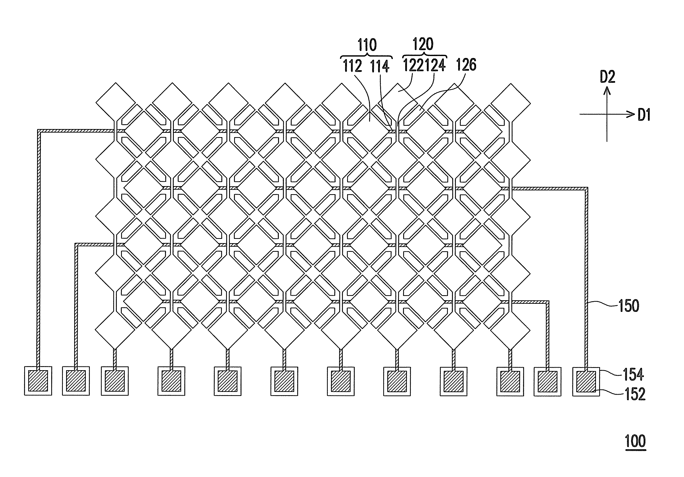
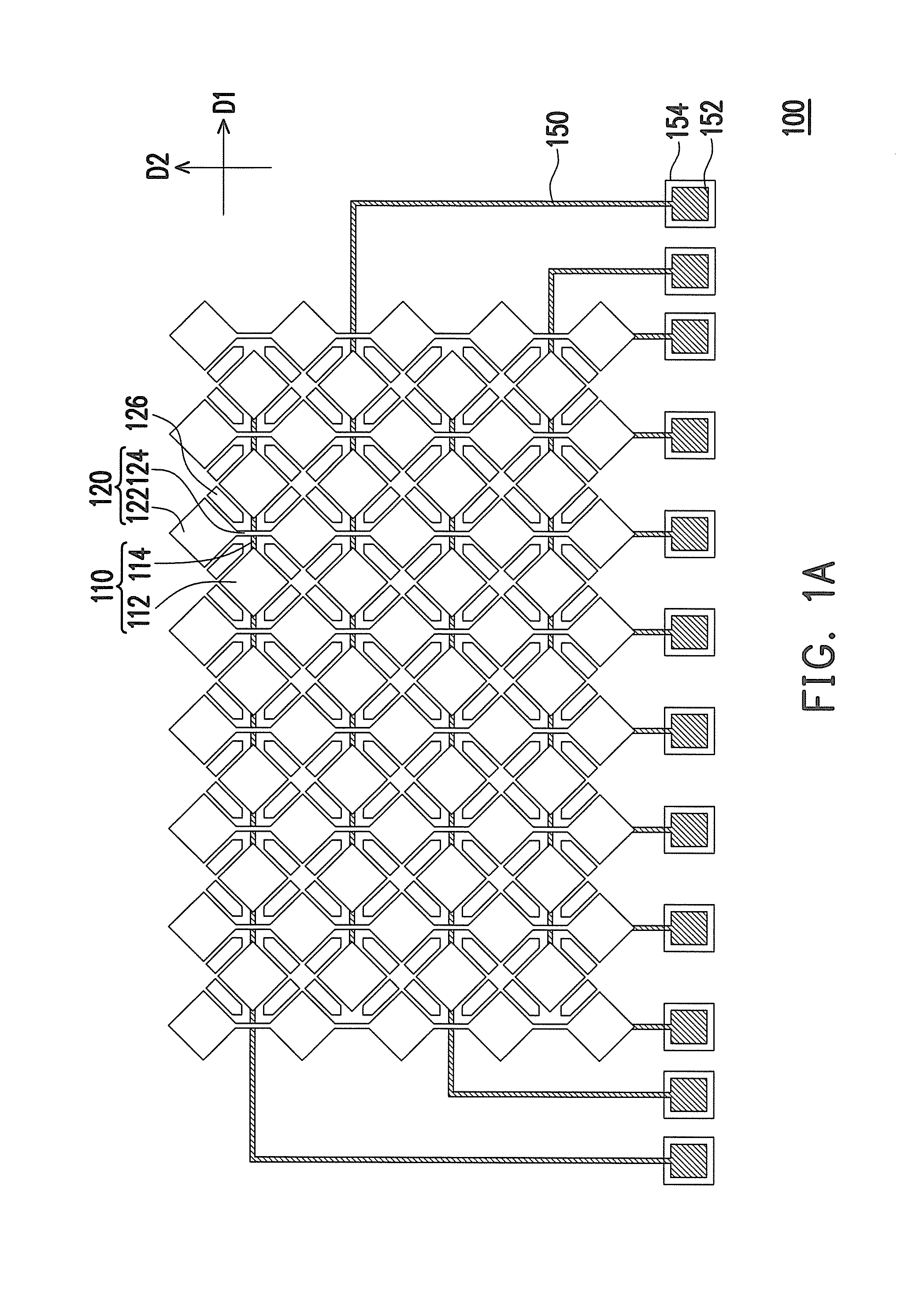
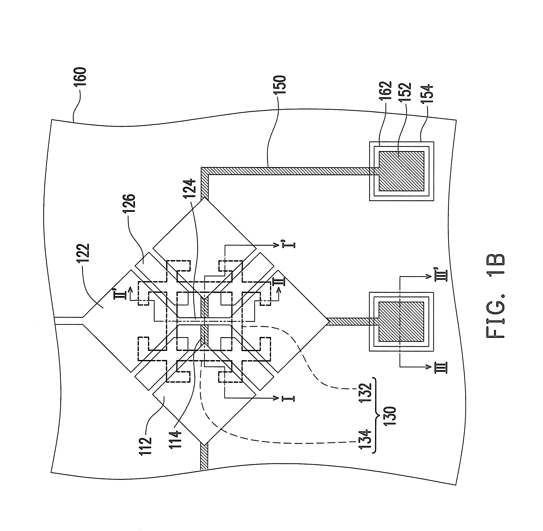
[0051]FIG. 1A is a schematic top view of a touch panel according to a first embodiment of the invention. FIG. 1B is a partially enlarged schematic diagram of FIG. 1A. FIG. 1C is schematic cross-sectional views taken along a line I-I′, a line II-II′, and a line III-III′ in FIG. 1B. Referring to FIG. 1A to FIG. 1C, in the embodiment, the touch panel 100 includes a substrate 102, a plurality of first sensing series 110, a plurality of the second sensing series 120, a plurality of conductive repairing pattern layers 130, and a first dielectric layer 140. The substrate 102 is, for example, a glass substrate, a plastic substrate, a flexible substrate, or other substrates. The substrate 102 can also be a printed circuit board or a display panel, such as a liquid crystal display panel, an organic display panel, an electrophoresis display panel, a plasma display panel, or other type display panels, and can directly assembly on the display panel or in the display panel. Ta...

second embodiment

The Second Embodiment

[0070]FIG. 6A is a schematic top view of a touch panel according to a second embodiment of the invention. FIG. 6B is a partially enlarged schematic diagram of FIG. 6A. FIG. 6C is schematic cross-sectional views taken along a line I-I′, a line II-II′, and a line III-III′ in FIG. 6B. Please simultaneously refer to FIG. 6A to FIG. 6C. In the embodiment, the touch panel 100 includes a substrate 102, a plurality of first sensing series 110, a plurality of the second sensing series 120, a plurality of conductive repairing pattern layers 130, a first dielectric layer 140, a second dielectric layer 160, a plurality of peripheral connecting lines 150, and a plurality of peripheral connecting pads 152. In the embodiment, the first dielectric layer 140 is, for example, disposed on the substrate 102, and includes a plurality of contact windows 142.

[0071]In the embodiment, the first sensing series 110 are disposed on the substrate 102 and extended along a first direction D1....


PUM

PropertyMeasurementUnit
conductiveaaaaaaaaaa
transparent conductiveaaaaaaaaaa
metallic conductiveaaaaaaaaaa

Abstract

A touch panel including a substrate, a plurality of first and second sensing series, and a plurality of conductive repairing pattern layers is provided. The first sensing series are disposed on the substrate and extended along a first direction. Each of the first sensing series includes a plurality of first sensing pads and first bridge lines, and the first bridge lines serially connect two adjacent first sensing pads. The second sensing series are disposed on the substrate and extended along a second direction. Each of the second sensing series includes a plurality of second sensing pads and second bridge lines, and the second bridge lines serially connect two adjacent second sensing pads. Each conductive repairing pattern layer electrically floating locates around the crossover region of the first and second sensing series. Two adjacent sensing pads are connected by the conductive repairing pattern layer after a repair procedure is finished.

Description

CROSS-REFERENCE TO RELATED APPLICATION[0001]This application claims the priority benefit of Taiwan application serial no. 99133743, filed on Oct. 4, 2010. The entirety of the above-mentioned patent application is hereby incorporated by reference herein and made a part of this specification.BACKGROUND OF THE INVENTION[0002]1. Field of the Invention[0003]The invention relates to a panel and a repairing method thereof, and more particularly to a touch panel and a repairing method thereof.[0004]2. Description of Related Art[0005]Based on different ways of sensing, touch panels are generally categorized into resistant touch panels, capacitive touch panels, optical touch panels, sonic wave touch panels, and electromagnetic touch panels. The capacitive touch panels having advantages of fast response speed, favorable reliability, and durability have been used extensively in electronic devices. In view of structures and manufacturing methods, capacitive touch display panels can be further cl...

Claims


Application Information

Patent Timeline
Patent Type & Authority Applications(United States)
IPC IPC(8): G06F3/041H01R43/00
CPCG06F3/044Y10T29/49117G06F2203/04111G06F3/0445G06F3/0446G06F3/047G06F2203/04103G06F2203/04112
Inventor CHAN, LIH-HSIUNGTSENG, SHINE-KAILIAO, CHIN-YUEHCHOU, HUNG-WEN
Owner AU OPTRONICS CORP
Why Eureka
Try Eureka