Method for producing surface emitting semiconductor device

Active Publication Date: 2012-04-19
SUMITOMO ELECTRIC IND LTD
View PDF5 Cites 7 Cited by
  • Summary
  • Abstract
  • Description
  • Claims
  • Application Information

AI Technical Summary

Benefits of technology

[0008]In order to reduce the influence of a stress caused by the lattice-mismatch in the oxidized regions 105c, the following method can be employed. Specifically, after the steps shown in FIGS. 12 to 14, an etching mask having a diameter slightly smaller than the diameter of the mesa portion 106 is formed on the mesa portion 106. A peripheral portion of the mesa portion 106 including the oxidized regions 105c is removed by a dry etching process using the etching mask. By employing this method, the oxidized regions 105c of the p-type DBR 105 are removed as shown in FIG. 16. Next, as shown in FIG. 17, an insulating film 107 and electrodes 108 and 109 are formed. According to this method, the oxidized regions 105c of the p-type DBR 105 can be removed, and the stress in the mesa portion 106 can be suppressed.
[0011]In this method, first, a semiconductor stacked structure including an active layer, a first semiconductor layer containing aluminum and provided on the active layer and, and a DBR portion provided on the first semiconductor layer is formed. The DBR portion includes second semiconductor layers and third semiconductor layers alternately stacked to each other. The second semiconductor layers and the third semiconductor layers of the DBR portion have different aluminum contents. A mesa portion is then formed by etching the DBR portion and the first semiconductor layer. Subsequently, the first semiconductor layer containing aluminum is oxidized from a side face of the mesa portion toward the inside of the mesa portion (oxidation step). In this oxidation step, an annular oxidized region for current confinement is formed inside the first semiconductor layer. In addition, the second semiconductor layers and the third semiconductor layers of the DBR portion are oxidized, and then an oxidized region is formed in the DBR portion. Subsequently, the oxidized region formed in the DBR portion is selectively etched by a wet etching (first etching step). In this first etching step, the oxidized region can be selectively etched and removed while suppressing etching of non-oxidized semiconductors. Subsequently, in a second etching step, a peripheral portion of the DBR portion is removed by etching, thereby adjusting the shape of the mesa portion without excessively etching the non-oxidized semiconductors of the mesa portion. According to the above method, since the oxidized region and the non-oxidized semiconductors can be separately etched by the most suitable methods, it is possible to prevent etching from reaching the substrate in the first etching step and the second etching step. As a result, a degradation of heat dissipation characteristics can be suppressed. In addition, since the oxidized region can be effectively removed, a decrease in reliability due to an internal stress can be suppressed. Furthermore, the DBR portion is configured by alternately stacking second semiconductor layers and third semiconductor layers having different aluminum contents. In the oxidation step, an oxidized region of each of the semiconductor layers having a high aluminum content, extends to the inner side of the DBR portion, as compared with an oxidized region of each of the semiconductor layers having a low aluminum content. Accordingly, in the first etching step, both the oxidized regions of the second semiconductor layers and the oxidized regions of the third semiconductor layers in the DBR portion can be effectively removed. After the first etching step, projections and recesses are formed on the side face of the DBR portion. These projections and recesses can be effectively eliminated in the second etching step.

Problems solved by technology

Cracks or dislocations may be formed in the mesa portion 106, resulting in a decrease in reliability of the device.
However, it was found that the following problem occurs, when this method is employed.
As a result, the device characteristics are also degraded.

Method used


Image

  • Method for producing surface emitting semiconductor device
  • Method for producing surface emitting semiconductor device
  • Method for producing surface emitting semiconductor device

Examples


Embodiment Construction

[0034]Embodiments of a method for producing a surface emitting semiconductor device according to the present invention will now be described in detail with reference to the accompanying drawings. In a description of the drawings, the same elements are assigned the same reference numerals and an overlapping description is omitted.

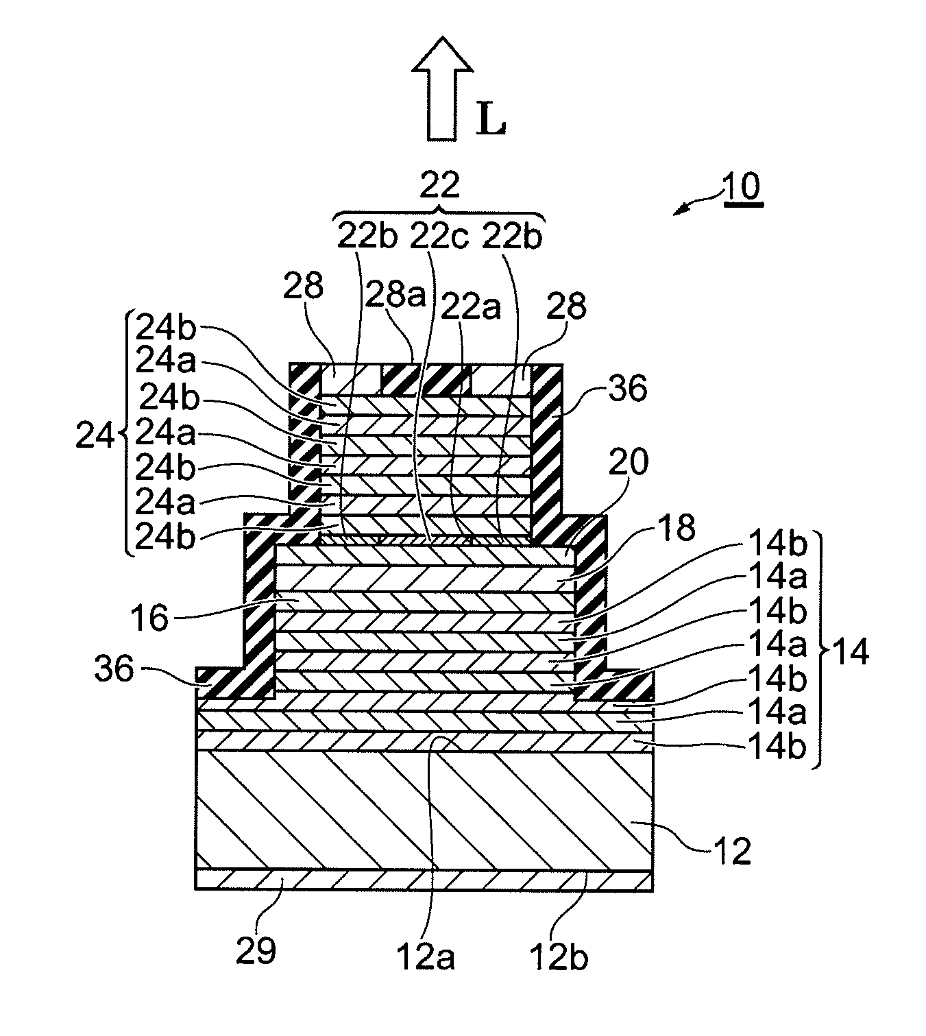
[0035]FIG. 1 is a cross-sectional side view of a surface emitting laser 10 which is an embodiment of a surface emitting semiconductor device produced by a method according to the present invention. The surface emitting laser 10 shown in FIG. 1 is a vertical cavity surface emitting laser (VCSEL), for example. In this embodiment, an emission direction of light L emitted from the surface emitting laser 10 is a direction perpendicular to a main surface 12a of a semiconductor substrate 12.

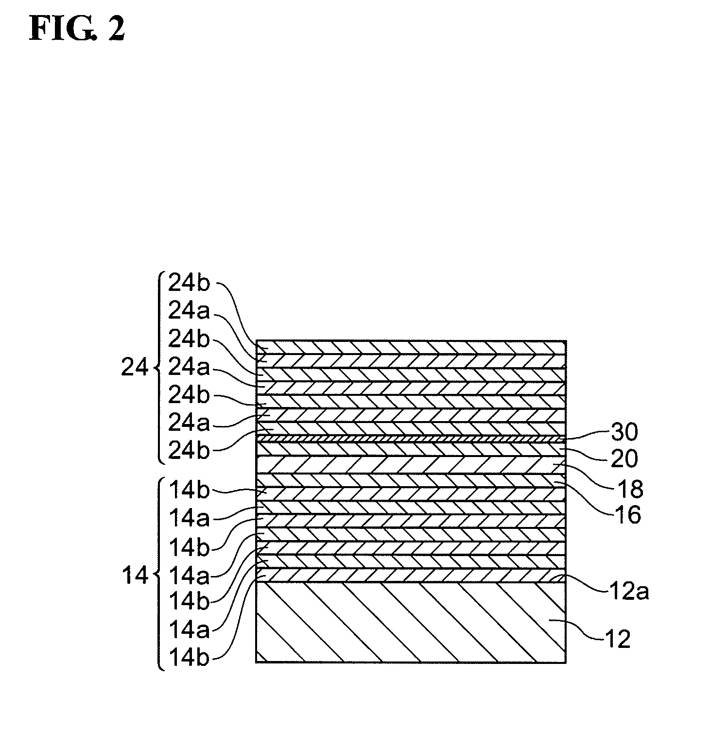
[0036]The surface emitting laser 10 includes a semiconductor substrate 12 of a first conductivity type, a first DBR portion 14 of the first conductivity type provided on the mai...


PUM


Abstract

A method for producing a surface emitting semiconductor device includes a step of forming a semiconductor stacked structure including an active layer, a first semiconductor layer containing aluminum on the active layer, and a DBR portion, on the first semiconductor layer, to include alternating stacked second semiconductor layers and third semiconductor layers having different aluminum contents; a step of forming a mesa portion by etching the DBR portion and the first semiconductor layer; an oxidation step of oxidizing the first semiconductor layer from a side face of the mesa portion toward the inside of the mesa portion to form an annular oxidized region inside the first semiconductor layer; a first etching step of selectively etching an oxidized region formed in the DBR portion; and a second etching step of removing a peripheral portion of the DBR portion.

Description

BACKGROUND OF THE INVENTION[0001]1. Field of the Invention[0002]The present invention relates to a method for producing a surface emitting semiconductor device.[0003]2. Description of the Related Art[0004]A vertical cavity surface emitting laser (VCSEL), for example, includes an active layer, a distributed Bragg reflector (DBR), and a current-confinement layer disposed between the active layer and the DBR. The current-confinement layer has a high-resistance region so as to confine a current in a center region surrounding the high-resistance region. For example, U.S. Pat. No. 6,570,905 describes a VCSEL formed on a GaAs substrate. In the VCSEL, an AlGaAs layer having a high aluminum content of 90% or more is used as a current-confinement layer.[0005]FIGS. 12 to 15 are cross-sectional views showing steps of producing such a VCSEL. First, as shown in FIG. 12, an n-type DBR 102, an active layer (multi quantum well (MQW) structure) 103, a spacer layer 110, a current-confinement layer 104...

Claims


Application Information

Patent Timeline
IPC IPC(8): H01L33/60
CPCH01L33/105H01S5/18311H01S5/2086H01S5/18394H01S5/18313
Inventor ONISHI, YUTAKA
Owner SUMITOMO ELECTRIC IND LTD
Why Eureka
Try Eureka