

Optical semiconductor apparatus
- Summary
- Abstract
- Description
- Claims
- Application Information
AI Technical Summary
Benefits of technology
Problems solved by technology
Method used
Image

Examples
example 1
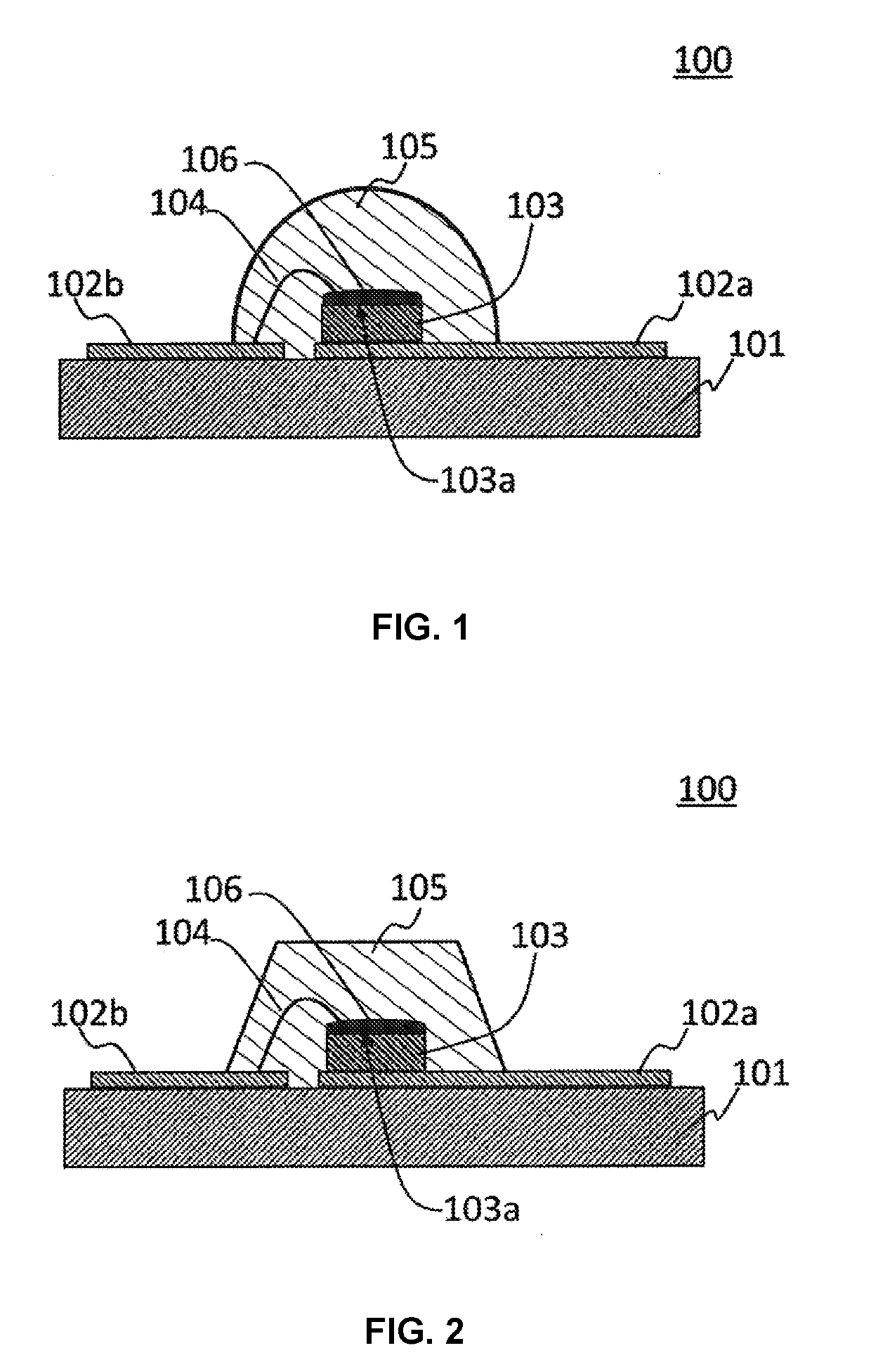
[0220]An ultraviolet LED with a configuration shown in FIG. 2 was prepared as follows.
[0221]1. Formation of Light-Permeable Buffer Layer
[0222]A buffer layer coating solution was prepared by diluting 8.00 g of the silicone resin composition B with 12.00 g of isopropanol.
[0223]After applying 100 nL of the buffer layer coating solution on a light-emitting surface 103a of a UV-LED die 103 (1.0 mm long, 1.0 mm wide, 0.1 mm thick) which had been arranged previously on a substrate to be electrically communicable using a dispenser, a light-permeable buffer layer 106 was formed through curing by keeping at room temperature 1 hour, at 70° C. for 1 hour and then at 150° C. for 1 hour. The light-permeable buffer layer 106 had a thickness of 15 μm as measured with LY-111 (Sony Magnescale) and had a smooth surface with no peeling, etc.
[0224]2. Formation of Flexible Sealing Layer
[0225]An ultraviolet LED 100 was prepared by forming a flexible sealing layer 105 with a truncated conical shape (top di...
examples 2-10
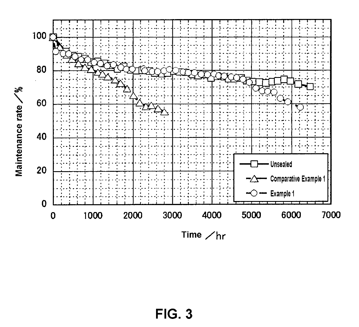
[0234]A sealed LED (ultraviolet LED 100 having light-permeable buffer layer 106 and flexible sealing layer 105) was prepared in the same manner as in Example 1, except that a light-permeable buffer layer 106 having a thickness described in Table 4 and having a smooth surface with no peeling, etc. was formed using the silicone resin composition described in Table 4 instead of the silicone resin composition B and a flexible sealing layer 105 was formed using the silicone resin composition described in Table 4 instead of the resin composition K10.
[0235]The sealed LED was evaluated in the same manner as in Example 1. The sealed LED showed no breakage of a wire 104.
[0236]The result is shown in Table 4.
PUM
| Property | Measurement | Unit |
|---|---|---|
| Temperature | aaaaa | aaaaa |
| Length | aaaaa | aaaaa |
| Volume | aaaaa | aaaaa |
Abstract
Description
Claims
Application Information