Electrostatic discharge protection device

a protection device and electrostatic discharge technology, applied in semiconductor devices, semiconductor/solid-state device details, diodes, etc., can solve the problems of chip failure, thermal breakdown of microchips, significant deterioration in the ability of ggdddnmos to cope with esd stress current, etc., to achieve high avalanche breakdown voltage and uniform operation of respective fingers

Inactive Publication Date: 2012-04-26
BAUABTECH
View PDF6 Cites 15 Cited by
  • Summary
  • Abstract
  • Description
  • Claims
  • Application Information

AI Technical Summary

Benefits of technology

[0010]The present disclosure provides improved electrostatic discharge protection devices that may have high avalanche breakdown voltage and cope with a large amount of electrostatic discharge current while achieving uniform operation of respective fingers in a multi-finger structure.

Problems solved by technology

Typically, chip failure occurs when static electricity caused by contact between an external pad of a microchip and a charged human body or machine is discharged to a core circuit or when accumulated static electricity flows to the core circuit.
Here, if the snapback phenomenon becomes too severe, the ESD protection device suffers a latch-up phenomenon which allows excess current to flow through the ESD protection device, thereby causing thermal breakdown of the microchip, even when the microchip is normally operated.
In such a GGDDDNMOS, however, a current path is mainly formed on the surface of the device, thereby causing a significant deterioration in the ability of the GGDDDNMOS to cope with ESD stress current.
Specifically, a surface temperature of the device sharply rises even at low current, causing thermal breakdown on the surface of the device at low current.
That is, as can be seen from the voltage-current characteristics of the GGDDDNMOS shown in FIG. 3, the GGDDDNMOS has low ability in coping with electrostatic current and a lower thermal breakdown voltage than the triggering voltage thereof, thereby making it difficult to achieve uniform operation of the respective fingers of the multi-finger structure.

Method used


Image

  • Electrostatic discharge protection device
  • Electrostatic discharge protection device
  • Electrostatic discharge protection device

Examples


Embodiment Construction

[0045]Exemplary embodiments will now be described in detail with reference to the accompanying drawings.

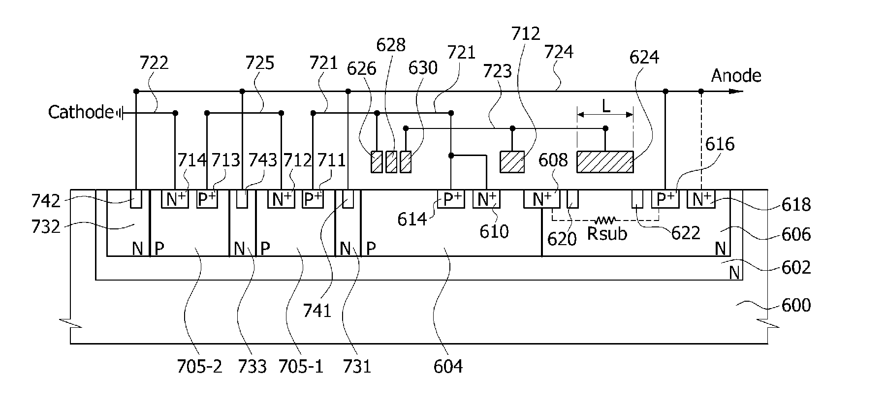
[0046]FIG. 4 is a diagram of an ESD protection device in accordance with one exemplary embodiment of the present disclosure. Referring to FIG. 4, an ESD protection device 400 includes a first group of electrostatic discharge protection devices 410 and a second group of electrostatic discharge protection devices 420 connected in series to each other between a first terminal T1 and a second terminal T2. The first group of electrostatic discharge protection devices 410 is connected in series to the first terminal T1 and includes at least one of a low on-resistance gate grounded rectifier (LORGGR) and a high on-resistance gate grounded rectifier (HORGGR). The second group of electrostatic discharge protection devices 420 is connected in series to the first group of electrostatic discharge protection devices 410 and the second terminal T2, and includes at least one of a gate grounded N...


PUM


Abstract

An ESD protection device is provided. The ESD protection device includes a first group of electrostatic discharge protection devices connected to a first terminal and including at least one of an LORGGR and an HORGGR, and a second group of electrostatic discharge protection devices connected in series to the first group of electrostatic discharge protection devices and a second terminal and including at least one of a GGNMOS, a GGPMOS and a diode.

Description

FIELD OF TECHNOLOGY[0001]The present disclosure relates to electrostatic discharge protection devices and, more particularly, to an electrostatic discharge protection device for high voltage operation.BACKGROUND[0002]Generally, in fabrication of microchips, it is an essential aspect of chip design to provide a circuit for protection of a microchip from electrostatic discharge (ESD) stress. Typically, chip failure occurs when static electricity caused by contact between an external pad of a microchip and a charged human body or machine is discharged to a core circuit or when accumulated static electricity flows to the core circuit. Here, a device used to protect the core circuit from such chip failure is referred to as an electrostatic discharge protection device. The electrostatic discharge protection device is generally disposed between the external pad and the core circuit.[0003]FIG. 1 is a graphical representation of fundamental requirements of an ESD protection device for a micr...

Claims


Application Information

Patent Timeline
Patent Type & Authority Applications(United States)
IPC IPC(8): H01L27/092
CPCH01L27/0629H01L27/0274
Inventor KIM, KILHO
Owner BAUABTECH
Why Eureka
Try Eureka