A high-side lateral double-diffused field-effect transistor

A technology of field effect transistor and lateral double diffusion, which is applied in the direction of semiconductor devices, electrical components, circuits, etc.

Active Publication Date: 2016-08-31
ZHEJIANG UNIV
View PDF4 Cites 0 Cited by
  • Summary
  • Abstract
  • Description
  • Claims
  • Application Information

AI Technical Summary

Problems solved by technology

Therefore, compared with the low-side LDMOS, there is another challenge in the structural design of the high-side LDMOS, that is, the high voltage between the source electrode and the substrate needs to be isolated to prevent breakdown and cause reliability such as noise and latch-up. question

Method used


Image

  • A high-side lateral double-diffused field-effect transistor
  • A high-side lateral double-diffused field-effect transistor
  • A high-side lateral double-diffused field-effect transistor

Examples


Embodiment Construction

[0014] In order to make the technical problems, technical solutions and improvement effects to be solved by the present invention clearer, the present invention will be further described in detail below in conjunction with the accompanying drawings.

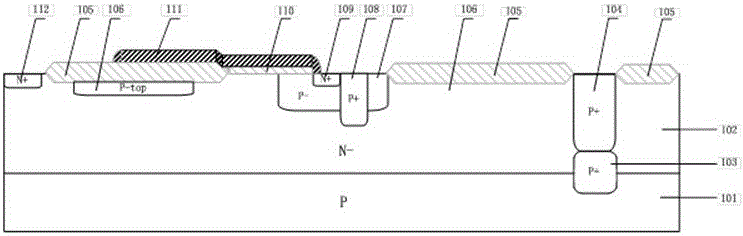
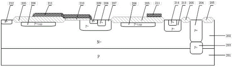
[0015] The high-side lateral double-diffused field-effect transistor structure of the present invention, such as figure 2 As shown, it includes: P-type substrate 201, N- epitaxial layer 202, P+ buried layer 203, P+ pair isolation 204, field oxygen 205, P-top layer 206, first P-body region 207 and second P- Body region 213 , the first P-body region contacts P+ 208 and the second P-body region contacts P+ 214 , N+ source electrode 209 , gate oxide layer 210 , polysilicon gate electrode 211 , and N+ drain electrode 212 .

[0016] The upper surface of the P-type substrate 201 is an N- epitaxial layer 202 . One side of the N- epitaxial layer 202 is provided with a P+ buried layer 203 and a P+ pair isolation 204 for isolating differe...


PUM


Abstract

The invention discloses a high-sided transverse double diffused field effect transistor. The high-sided transverse double diffused field effect transistor comprises a P type substrate, an N- epitaxial layer, a P+ buried layer, a P+ P-N junction isolation, field oxygen, a P- top layer, P- body areas, a P- body area contact P+, an N+ source electrode, a gate oxygen layer, a polycrystalline silicon gate electrode and an N+ drain electrode, wherein the N- epitaxial layer is arranged above the P type substrate; the P+ buried layer and the P+ P-N junction isolation are arranged at one side of the N- epitaxial layer and are used to isolate different types of devices; furthermore, another P- body area is arranged between the P- body area and the P+ P-N junction isolation; the body area contact P+ is arranged in the P- body area; the P- top layer is arranged between the P- body area and the another P- body area. According to the high-sided transverse double diffused field effect transistor disclosed by the invention, an avalanche breakdown voltage between the source electrode and the substrate is greatly increased, that is, an isolation performance is greatly improved, so that application in the field which requires relatively high working voltage is satisfied.

Description

technical field [0001] The invention relates to the field of semiconductor power devices, in particular to a high-side lateral double-diffused field-effect transistor (LDMOS). Background technique [0002] Power integrated circuit PIC (Power Integrated Circuit) is a special integrated circuit that integrates power devices, control circuits, signal processing circuits, etc. into the same chip. As a branch of integrated circuits, PIC has always played a vital role. Compared with discrete devices, PIC not only has great advantages in terms of circuit performance, stability and power consumption, but also has great potential in reducing costs, reducing volume and weight. Because of these advantages, PIC is widely used in many application fields such as computer, communication and network, consumer electronics, industrial control and automotive electronics. The lateral double-diffused metal-oxide semiconductor (LDMOS) is widely used in power integrated circuit drive output stag...

Claims


Application Information

Patent Timeline
Patent Type & Authority Patents(China)
IPC IPC(8): H01L29/78H01L29/06
CPCH01L29/0634H01L29/7816
Inventor 吴焕挺韩雁张世峰张炜
Owner ZHEJIANG UNIV
Why Eureka
Try Eureka