SiGe-heterojunction bipolar transistor (HBT) and preparation method thereof

A technology of transistors and conductors, applied in the field of SiGe heterojunction bipolar transistors and its preparation, can solve the problems of lower characteristic frequency, deterioration of breakdown voltage, increase of doping concentration in collector area, etc., to improve fT and reduce ionization The probability of collision and the effect of increasing the characteristic frequency

Inactive Publication Date: 2014-08-27
SHANGHAI INST OF MICROSYSTEM & INFORMATION TECH CHINESE ACAD OF SCI
View PDF5 Cites 0 Cited by
  • Summary
  • Abstract
  • Description
  • Claims
  • Application Information

AI Technical Summary

Problems solved by technology

[0008] In view of the above-mentioned shortcoming of prior art, the object of the present invention is to provide a kind of SiGe-HBT transistor and preparation method thereof, be used for solving prior art, when raising base-collector breakdown voltage, cause characteristic frequency to reduce , or the problem of breakdown voltage deterioration caused by increasing the doping concentration of the collector region, increasing the characteristic frequency, and increasing the transit time of the space charge region

Method used


Image

  • SiGe-heterojunction bipolar transistor (HBT) and preparation method thereof
  • SiGe-heterojunction bipolar transistor (HBT) and preparation method thereof
  • SiGe-heterojunction bipolar transistor (HBT) and preparation method thereof

Examples


Embodiment 1

[0059] Control attached Figure 2a-2d A further explanation and illustration is made on the preparation method of a SiGe-HBT transistor provided by the present invention.

[0060] First, if Figure 2a The structures shown were prepared using conventional techniques known to those skilled in the art, and the materials described were conventional materials well known to those skilled in the art. For example, a general SiGe heterojunction double transistor is fabricated on a semiconductor substrate (not shown in the figure), and the substrate material is selected from one of Si, Ge, and GeSi, but not limited to these materials. The substrate can be an N-type or P-type substrate, depending on the type of device being fabricated.

[0061] exist Figure 2a The structure in includes a sub-collector region 11 formed on a semiconductor substrate (not shown in the figure), and the sub-collector region 11 is formed by a conventional ion implantation or epitaxial growth process, and th...

Embodiment 2

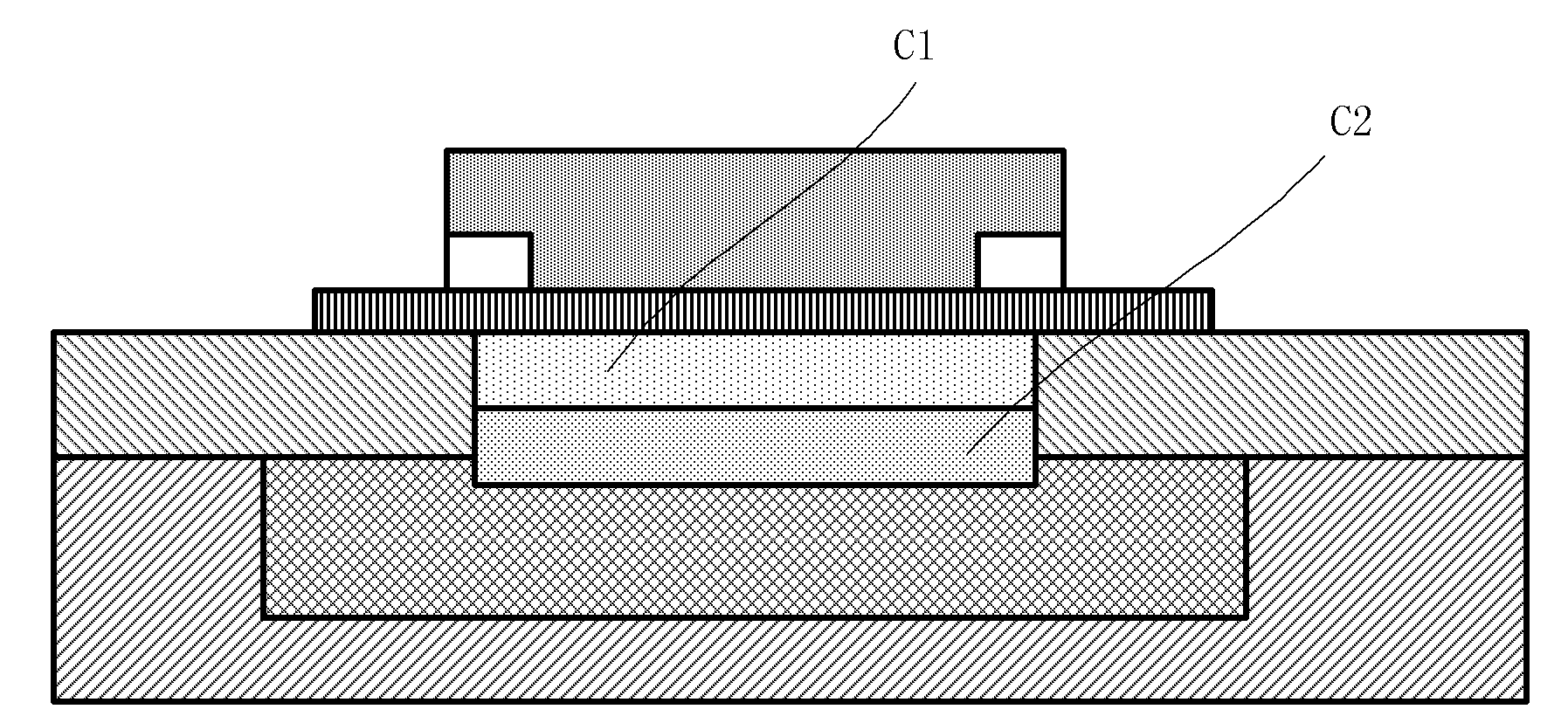
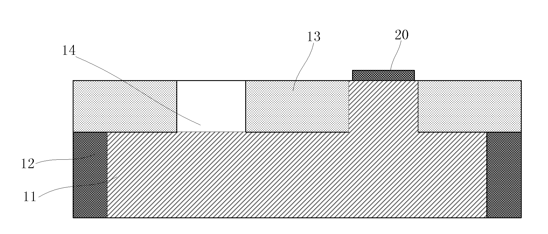
[0076] The present invention also provides a SiGe-HBT transistor structure, such as Figure 2d shown, including:

[0077] The sub-collector region 11 isolated by the deep trench isolation 12, and the collector region 14 formed on the sub-collector region 11 and isolated by the shallow trench isolation region 13, and the collector region is formed on the sub-collector region Electrode contacts 20 .

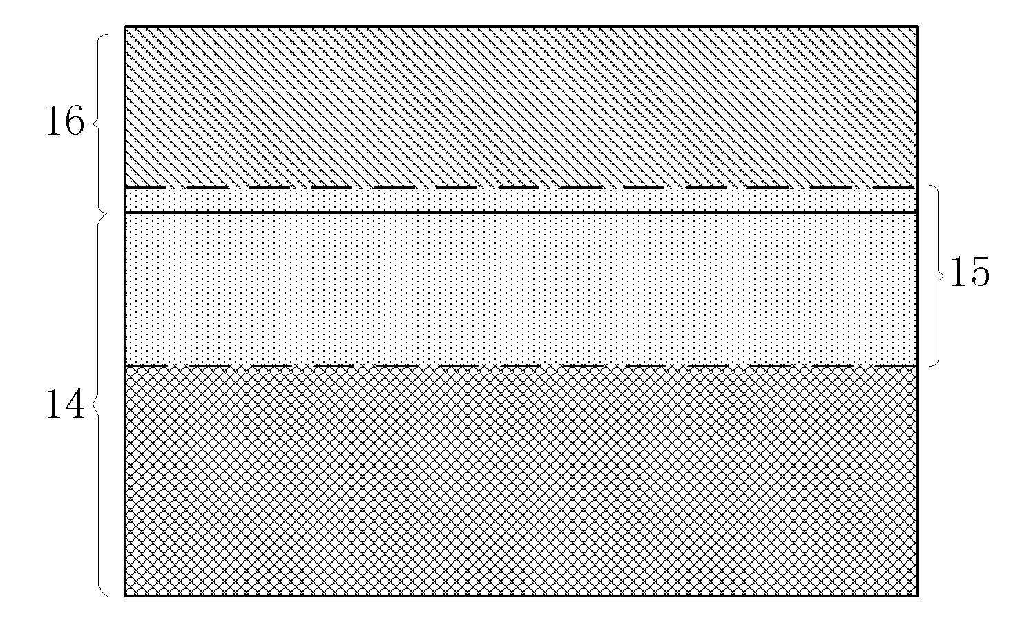
[0078] The base region 16 is formed on the collector region 14 and the shallow trench isolation region 13, including an intrinsic SiGe layer 160, heavily doped P + The polysilicon outer base layer 162 and the intrinsic SiGe layer 160 and heavily doped P + The base region P-SiGe:C layer 161 between the polysilicon outer base region layers 162, the contact interface of the collector region 14 and the base region 16 is formed with a collector-base junction space charge region 15, and the P + A base contact 21 is formed on the polysilicon outer base layer 162 .

[0079] emitter reg...


PUM


Abstract

The present invention provides a SiGe-heterojunction bipolar transistor (HBT) and a manufacturing method thereof, and belongs to the field of microelectronics and solid-state electronics. According to the manufacturing method for the SiGe-HBT, by adopting an ion implantation technology, a stacked layer consisting of a P+ layer and an N+ layer with same dosage concentration is formed in an overlapped zone of a collector region and space charge region. The doping concentration of the P+ layer or N+ layer is in Gaussian distribution, and is less than the doping concentration of a base region while greater than the doping concentration of the collector region. According to the solution of the present invention, not only the value of the electric field of a partial barrier region, but also the distribution of the electric field of the barrier region can be changed; the base-collector breakdown voltage is increased without sacrificing the transit time, the cut-off frequency and the maximum oscillation frequency; or the doping concentration of the collector region, the transit time and the cut-off frequency of the space charge region are increased without worsening the breakdown ­voltage.

Description

technical field [0001] The invention relates to the technical field of microelectronics and solid electronics, in particular to a SiGe heterojunction bipolar transistor (SiGe-HBT) and a preparation method thereof. Background technique [0002] The heterojunction bipolar transistor (HBT) fundamentally overcomes the inherent contradiction of conventional bipolar junction transistors (Bipolar Junction Transistor, BJT) by using energy band engineering, that is, the contradiction between increasing the amplification factor and increasing the characteristic frequency, so HBT can achieve ultra-high frequency and ultra-high speed. Moreover, SiGe technology is fully compatible with advanced CMOS technology, so SiGe-BiCMOS technology has been formed, which accordingly promotes the rapid development of microwave and radio frequency communication technologies. [0003] However, there are many physical characteristics affecting HBT devices: Early effect (related to bias), high injection...

Claims


Application Information

Patent Timeline
Patent Type & Authority Patents(China)
IPC IPC(8): H01L21/331H01L29/737H01L29/06
CPCH01L29/0821H01L29/7378
Inventor 陈静余涛罗杰馨伍青青柴展
Owner SHANGHAI INST OF MICROSYSTEM & INFORMATION TECH CHINESE ACAD OF SCI
Why Eureka
Try Eureka