A planar mercury cadmium telluride avalanche diode detector and its preparation method

An avalanche diode and mercury cadmium telluride technology, which is applied in the field of infrared detectors, can solve the problems of limiting the effective working bias range and gain range, and achieve the effects of increasing the avalanche breakdown voltage, reducing the electric field strength, and increasing the width

Active Publication Date: 2021-09-03
11TH RES INST OF CHINA ELECTRONICS TECH GROUP CORP
View PDF0 Cites 0 Cited by
  • Summary
  • Abstract
  • Description
  • Claims
  • Application Information

AI Technical Summary

Problems solved by technology

The actual PN junction can be divided into three parts: the horizontal cylindrical junction, the vertical planar junction, and the spherical junction at the corner. Since the curvature radius of the cylindrical junction and the spherical junction is smaller than that of the planar junction, the cylindrical junction and the spherical junction The electric field at the junction is seriously concentrated, so that the tunneling current associated with the electric field at the cylindrical and spherical junctions is much higher than that at the planar junction, and the avalanche breakdown voltage at the cylindrical and spherical junctions is lower than The avalanche breakdown voltage at the planar junction limits the effective operating bias range and corresponding gain range of HgCdA avalanche diode detectors in linear mode

Method used


Image

  • A planar mercury cadmium telluride avalanche diode detector and its preparation method
  • A planar mercury cadmium telluride avalanche diode detector and its preparation method
  • A planar mercury cadmium telluride avalanche diode detector and its preparation method

Examples


preparation example Construction

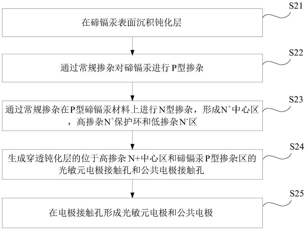
[0035] Such as figure 2 As shown, it is a schematic diagram of the implementation process of the method for preparing a planar mercury cadmium telluride avalanche diode detector provided by the embodiment of the present invention, including the following steps:

[0036] S21. Depositing a passivation layer on the surface of HgCdTe.

[0037] During specific implementation, a passivation layer of cadmium telluride is deposited on the surface of mercury cadmium telluride; or cadmium telluride and zinc sulfide are sequentially deposited on the surface of mercury cadmium telluride to form the passivation layer.

[0038] Wherein, the thickness of the cadmium telluride layer can be 30-500 nm, and the thickness of the zinc sulfide layer can be 0-500 nm.

[0039] S22 , performing P-type doping on HgCdTe by conventional doping.

[0040] Among them, the concentration of HgCdTe P-type doped region can be: 5e15cm -3 ~5e16cm -3 .

[0041] S23. Perform N-type doping on the P-type HgCdTe...


PUM

PropertyMeasurementUnit
thicknessaaaaaaaaaa
thicknessaaaaaaaaaa
thicknessaaaaaaaaaa

Abstract

The present invention proposes a planar mercury cadmium telluride avalanche diode detector and its preparation method, which are used to reduce the electric field intensity in the cylindrical junction and spherical junction depletion region of the planar mercury cadmium telluride avalanche diode detector, thereby reducing the corresponding tunneling current, increase the avalanche breakdown voltage, and increase the gain in linear mode. The method includes: depositing a passivation layer on the surface of HgCdTe; performing P-type doping on HgCdTe through conventional doping; performing N-type doping on P-type HgCdTe materials through conventional doping to form N + Central region, highly doped N + guard ring and low doping N ‑ region; generate a penetrating passivation layer located in a highly doped N + The photosensitive element electrode contact hole and the common electrode contact hole of the central area and the HgCdTe P-type doped area; the photosensitive element electrode and the common electrode are formed in the electrode contact hole.

Description

technical field [0001] The invention relates to the technical field of infrared detectors, in particular to a planar mercury cadmium telluride avalanche diode detector and a preparation method thereof. Background technique [0002] HgCdTe avalanche diode detectors can work in Geiger mode and linear mode respectively according to different working bias voltages. In Geiger mode, the working bias voltage of the HgCdTe avalanche diode detector is higher than the avalanche breakdown voltage, and the output signal amplitude has nothing to do with the received photoelectric signal amplitude, which requires an external circuit to quench the detector before The next signal detection; in the linear mode, the working bias of the mercury cadmium telluride avalanche diode detector is lower than the avalanche breakdown voltage, the gain of the mercury cadmium telluride avalanche diode detector changes with the bias voltage, and the received photoelectric signal can be processed High-spee...

Claims


Application Information

Patent Timeline
Patent Type & Authority Patents(China)
IPC IPC(8): H01L31/107H01L31/18
CPCH01L31/107H01L31/18H01L31/1876Y02P70/50
Inventor 张智超喻松林张轶
Owner 11TH RES INST OF CHINA ELECTRONICS TECH GROUP CORP
Why Eureka
Try Eureka