Eureka AIR delivers breakthrough ideas for toughest innovation challenges, trusted by R&D personnel around the world.

Liquid crystal display device

Inactive Publication Date: 2012-04-26
PANASONIC LIQUID CRYSTAL DISPLAY CO LTD +1
View PDF1 Cites 14 Cited by
  • Summary
  • Abstract
  • Description
  • Claims
  • Application Information

AI Technical Summary

Benefits of technology

[0007]In the liquid crystal display device disclosed in Japanese Patent Application Laid-open No. 2008-276172, the number of ends of slits is reduced by providing the slits so as to extend continuously over a plurality of pixels. In other words, in the liquid crystal display device, the domain is reduced by reducing the number of ends of slits which are responsible for generation of the domain.
[0009]The present invention has been made in view of the above, and an object of the present invention is to provide a liquid crystal display device which improves the transmittance.
[0024]In the liquid crystal display device according to the present invention in which the pixel electrode and the common electrode are stacked via the insulating layer, the slits are formed in one of the pixel electrode and the common electrode, and the liquid crystal molecules are aligned by an electric field generated by the pixel electrode and the common electrode, the insulating layer is formed so as to increase in thickness from the vicinity of the ends in the longitudinal direction of the slits toward the ends, to thereby lower the intensity of the electric field in the vicinity of the ends in the longitudinal direction of the slits. Because of the lowered intensity of the electric field, the liquid crystal molecules are normally aligned around the ends in the longitudinal direction of the slits and thus suppress enlargement of a domain which is generated by the electric field in the vicinity of the ends in the longitudinal direction of the slits. Therefore, the domain reduces, and, as a consequence, the transmittance may be improved.
[0025]Further, in the liquid crystal display device according to the present invention in which the pixel electrode and the common electrode are stacked via the insulating layer, the slits are formed in one of the pixel electrode and the common electrode, and the liquid crystal molecules are aligned by an electric field generated by the pixel electrode and the common electrode, the slits are formed so as to be inflected, and the insulating layer is formed so as to increase in thickness from the vicinity of the inflected portions of the slits toward the inflected portions, to thereby lower the intensity of the electric field in the vicinity of the inflected portions of the slits. Because of the lowered intensity of the electric field, the liquid crystal molecules are normally aligned around the inflected portions of the slits and thus suppress enlargement of a domain which is generated by the electric field in the vicinity of the inflected portions of the slits. Therefore, the domain reduces, and, as a consequence, the transmittance may be improved.
[0026]Further, in the liquid crystal display device according to the present invention in which the pixel electrode and the common electrode are stacked via the insulating layer, the slits are formed in one of the pixel electrode and the common electrode, and the liquid crystal molecules are aligned by an electric field generated by the pixel electrode and the common electrode, the slits are formed so as to be inflected, the insulating layer is formed so as to increase in thickness from the ends in the longitudinal direction of the slits toward the ends, and the insulating layer is formed so as to increase in thickness from the vicinity of the inflected portions of the slits toward the inflected portions, to thereby lower the intensity of the electric field in the vicinity of the ends in the longitudinal direction of the slits and in the vicinity of the inflected portions. Because of the lowered intensity of the electric field, the liquid crystal molecules are normally aligned around the ends in the longitudinal direction of the slits and around the inflected portions and thus suppress enlargement of a domain which is generated by the electric field in the vicinity of the ends in the longitudinal direction of the slits and in the vicinity of the inflected portions. Therefore, the domain reduces, and, as a consequence, the transmittance may be improved.

Problems solved by technology

However, in the liquid crystal display device disclosed in Japanese Patent Application Laid-open No. 2008-276172, not all the ends of slits are eliminated, and thus, the problem that a domain generated in the vicinity of ends of slits lowers the transmittance is not solved.

Method used


Image

  • Liquid crystal display device
  • Liquid crystal display device
  • Liquid crystal display device

Examples


first embodiment

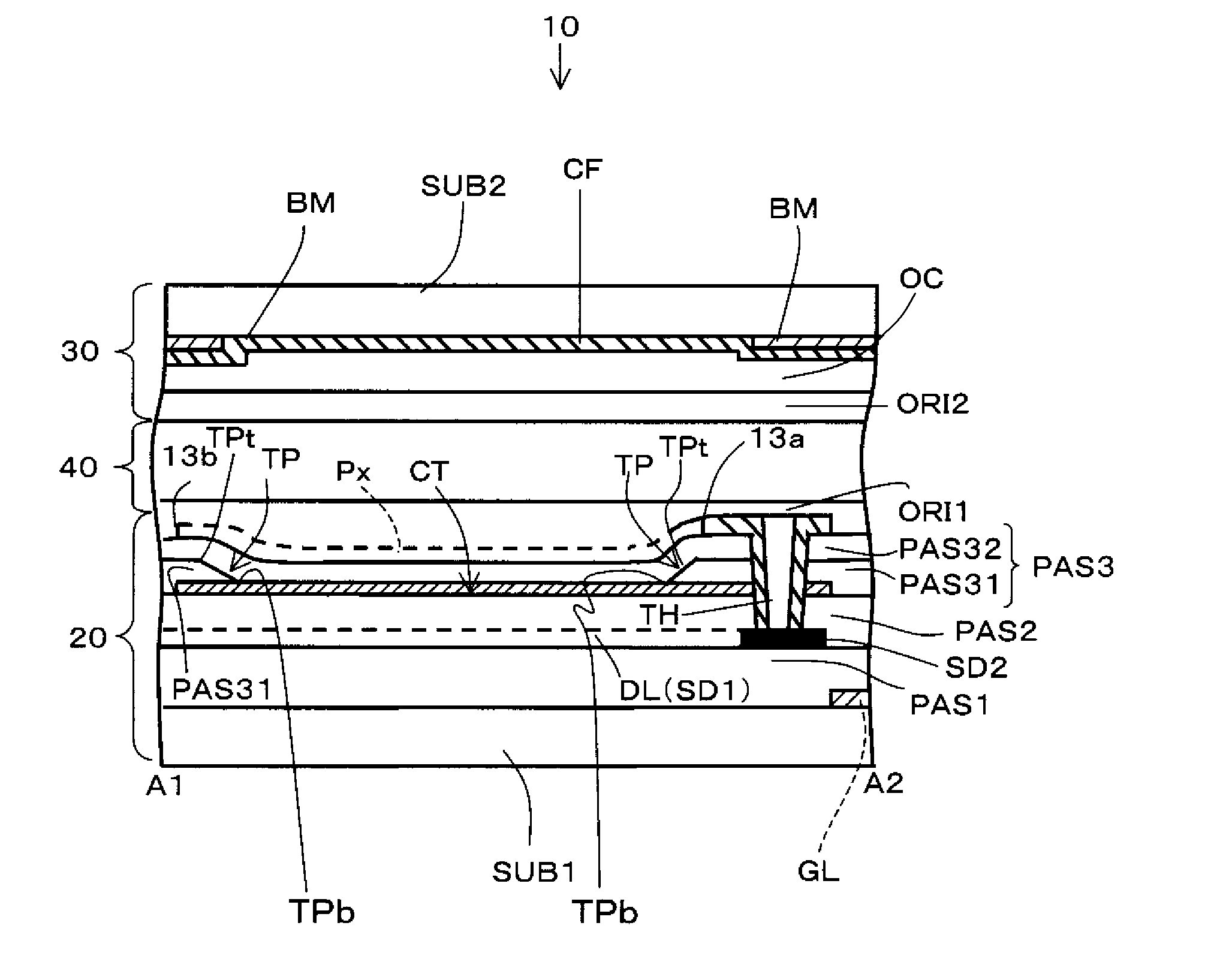
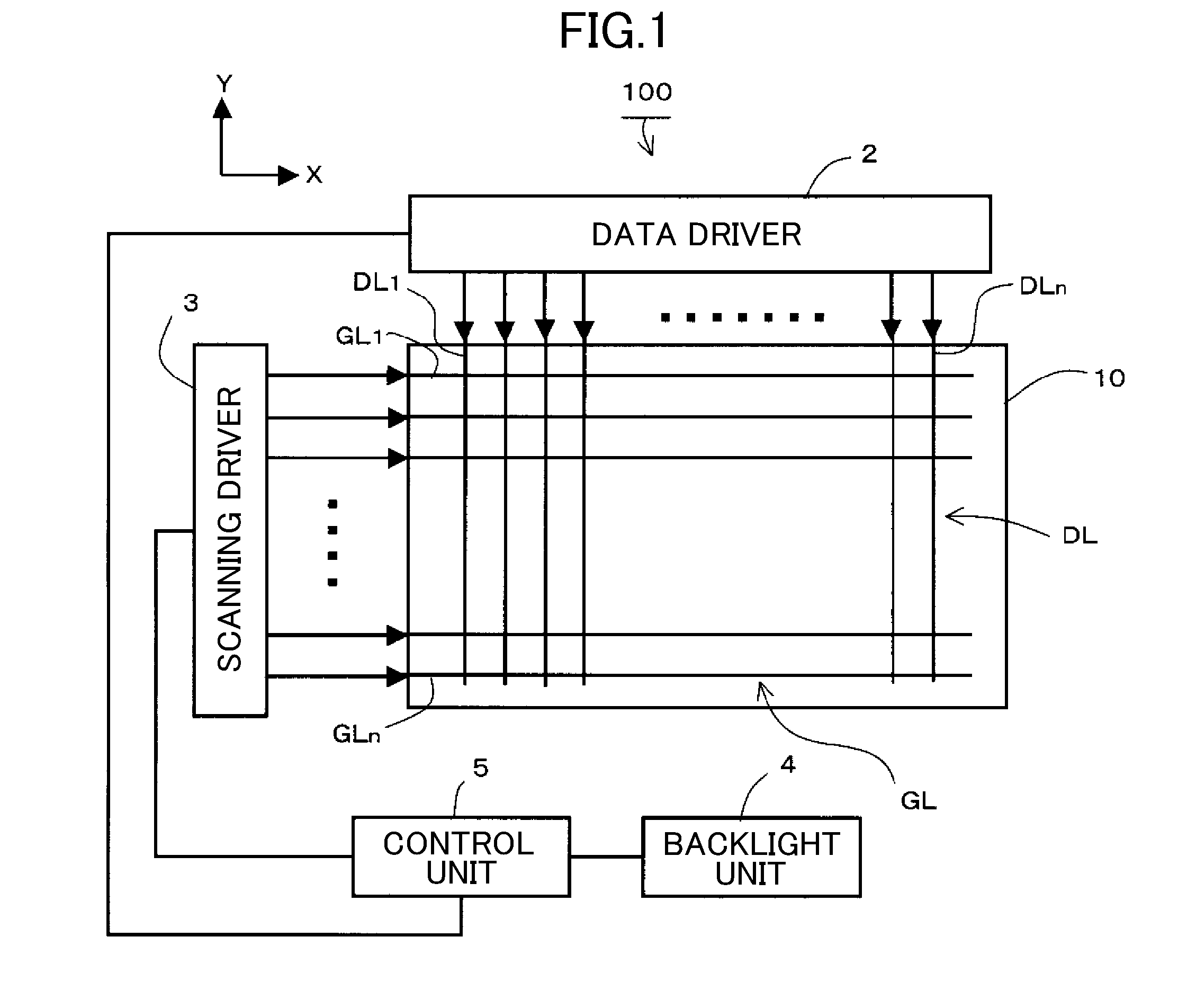
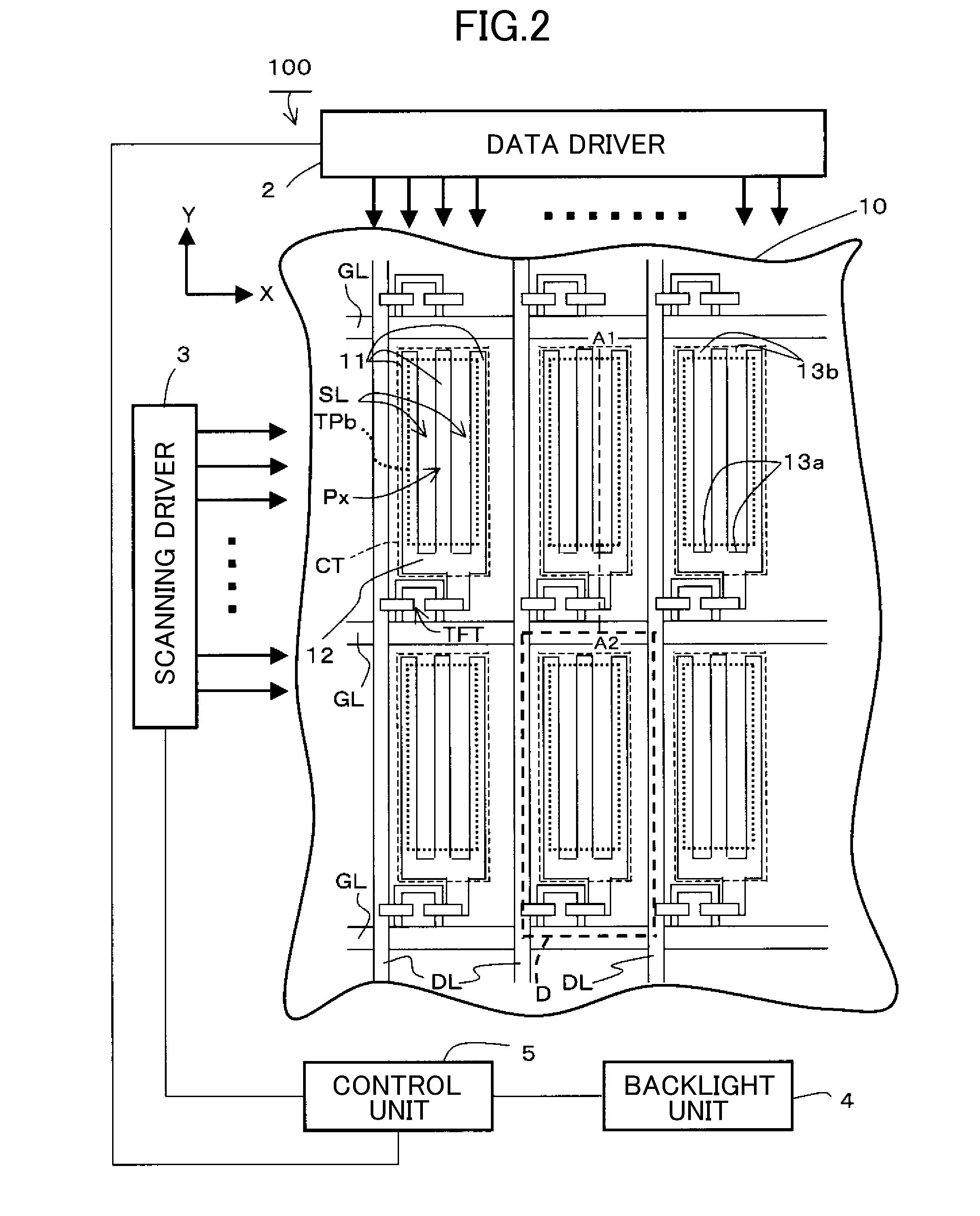
[0038]FIG. 1 is a schematic view illustrating a structure of a liquid crystal display device 100 according to a first embodiment of the present invention. FIG. 2 is a detailed explanatory diagram of a structure of a liquid crystal display panel 10 illustrated in FIG. 1. In FIG. 2, the part of a liquid crystal display panel 10 is enlarged to explain the structure of pixels. FIG. 3 is a cross-sectional view of the liquid crystal display panel 10 taken along the line A1-A2 of FIG. 2. The liquid crystal display device 100 is of the horizontal electric field system, and includes the liquid crystal display panel 10, a data driver 2, a scanning driver 3, a backlight unit 4, and a control unit 5.

[0039]As illustrated in FIG. 1, the liquid crystal display panel 10 includes a plurality of video signal lines DL (DL1, . . . , DLn, where n is a natural number) which extend in a Y direction and a plurality of scanning signal lines GL (GL1, . . . , GLm, where m is a natural number) which extend in ...

second embodiment

[0059]Next, a second embodiment of the present invention is described with reference to FIG. 4 and FIG. 5. FIG. 4 is a detailed explanatory diagram of a structure of a liquid crystal display panel 60 of a liquid crystal display device 200 according to the second embodiment of the present invention. FIG. 5 is a cross-sectional view of the liquid crystal display panel 60 taken along the line B1-B2-B3 of FIG. 4. In the first embodiment of the present invention, the slits SL are in the shape of straight lines, but, in the second embodiment, the slits SL each have a inflected portion 13c. The third insulating layer PAS3 is formed so as to gradually increase in thickness from the vicinity of the inflected portions 13c toward the inflected portions 13c. Other structures in the second embodiment are the same as those in the first embodiment, and like reference symbols are used to designate like structural elements.

[0060]As illustrated in FIG. 4, a pixel electrode Px has a plurality of strip...

third embodiment

[0068]Next, a third embodiment of the present invention is described with reference to FIG. 6 and FIG. 7. FIG. 6 is a detailed explanatory diagram of a structure of a liquid crystal display panel 70 of a liquid crystal display device 300 according to the third embodiment of the present invention. FIG. 7 is a cross-sectional view of the liquid crystal display panel 70 taken along the line C1-C2-C3 of FIG. 6. In the second embodiment of the present invention, the third insulating layer PAS3 is formed so as to gradually increase in thickness from the vicinity of the inflected portions 13c toward the inflected portions 13c. In the third embodiment, further, the third insulating layer PAS3 is formed so as to gradually increase in thickness from the vicinity of the closed ends 13a toward the closed ends 13a and is formed so as to gradually increase in thickness from the vicinity of the open ends 13b toward the open ends 13b. Other structures in the third embodiment are the same as those i...


PUM


Abstract

Provided is a liquid crystal display device (100), including a pixel electrode (Px) and a common electrode (CT) which are stacked via an insulating layer, one of the pixel electrode (Px) and the common electrode (CT) including slits (SL) formed therein, for aligning liquid crystal molecules by an electric field generated by the pixel electrode (Px) and the common electrode (CT), in which the insulating layer is formed so as to increase in thickness from a vicinity of ends (13a, 13b) in a longitudinal direction of the slits (SL) toward the ends (13a, 13b). Thus, the transmittance of the liquid crystal display device is improved.

Description

CROSS-REFERENCE TO RELATED APPLICATION[0001]The present application claims priority from Japanese application JP 2010-236077 filed on Oct. 21, 2010, the content of which is hereby incorporated by reference into this application.BACKGROUND OF THE INVENTION[0002]1. Field of the Invention[0003]The present invention relates to a liquid crystal display device in which liquid crystal molecules are aligned by an electric field generated by two electrodes stacked via an insulating layer.[0004]2. Description of the Related Art[0005]Conventionally, liquid crystal display devices are classified into ones of a vertical electric field system and ones of a horizontal electric field system. A liquid crystal display device of the horizontal electric field system may obtain wider viewing angle characteristics compared with those of a liquid crystal display device of the vertical electric field system. Among liquid crystal display devices of the horizontal electric field system, ones in which a pixel...

Claims


Application Information

Patent Timeline
IPC IPC(8): G02F1/1343
CPCG02F2001/134372G02F1/133345G02F1/134372
Inventor OUGIICHI, KIMITOSHIIMAYAMA, HIROTAKA
Owner PANASONIC LIQUID CRYSTAL DISPLAY CO LTD
Why Eureka
Eureka Blog
Learn More