Semiconductor light emitting device and method for manufacturing the same

Active Publication Date: 2009-05-28
MITSUBISHI ELECTRIC CORP
View PDF1 Cites 4 Cited by
  • Summary
  • Abstract
  • Description
  • Claims
  • Application Information

AI Technical Summary

Benefits of technology

[0010]In the optical pickup, when the variation of the polarizing angle relative to change in the operating environment temperature of the semiconductor laser is larger, the combining efficiency of optical parts and laser beams is lowered, more optical output is required on data writing, and power consumption is increased. Therefore, the variation of the polarizing angle relative to change in the operating environment temperature must be small.
[0013]To solve the above-described problems, it is an object of the present invention to provide a semiconductor light emitting device that can reduce the polarizing angle of a laser, and a method for manufacturing such a semiconductor light emitting device.
[0015]According to the present invention, the polarizing angle of a laser can be reduced.

Problems solved by technology

However, residual stress could not be sufficiently lowered in conventional semiconductor light emitting device.
In the optical pickup, when the variation of the polarizing angle relative to change in the operating environment temperature of the semiconductor laser is larger, the combining efficiency of optical parts and laser beams is lowered, more optical output is required on data writing, and power consumption is increased.
In conventional semiconductor light emitting devices, however, the polarizing angle of a laser was large due to the effect of residual stress, and the variation of the polarizing angle relative to change in the operating environment temperature was large.
Therefore, there were problems wherein the yield in the test was poor, and the operation of the semiconductor laser was unstable.

Method used


Image

  • Semiconductor light emitting device and method for manufacturing the same
  • Semiconductor light emitting device and method for manufacturing the same
  • Semiconductor light emitting device and method for manufacturing the same

Examples


first embodiment

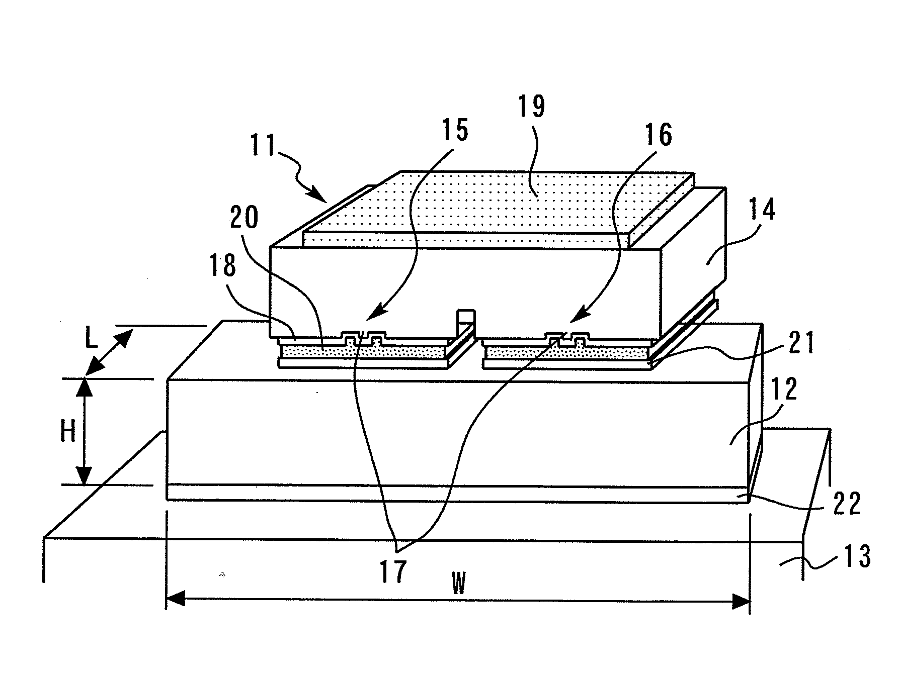
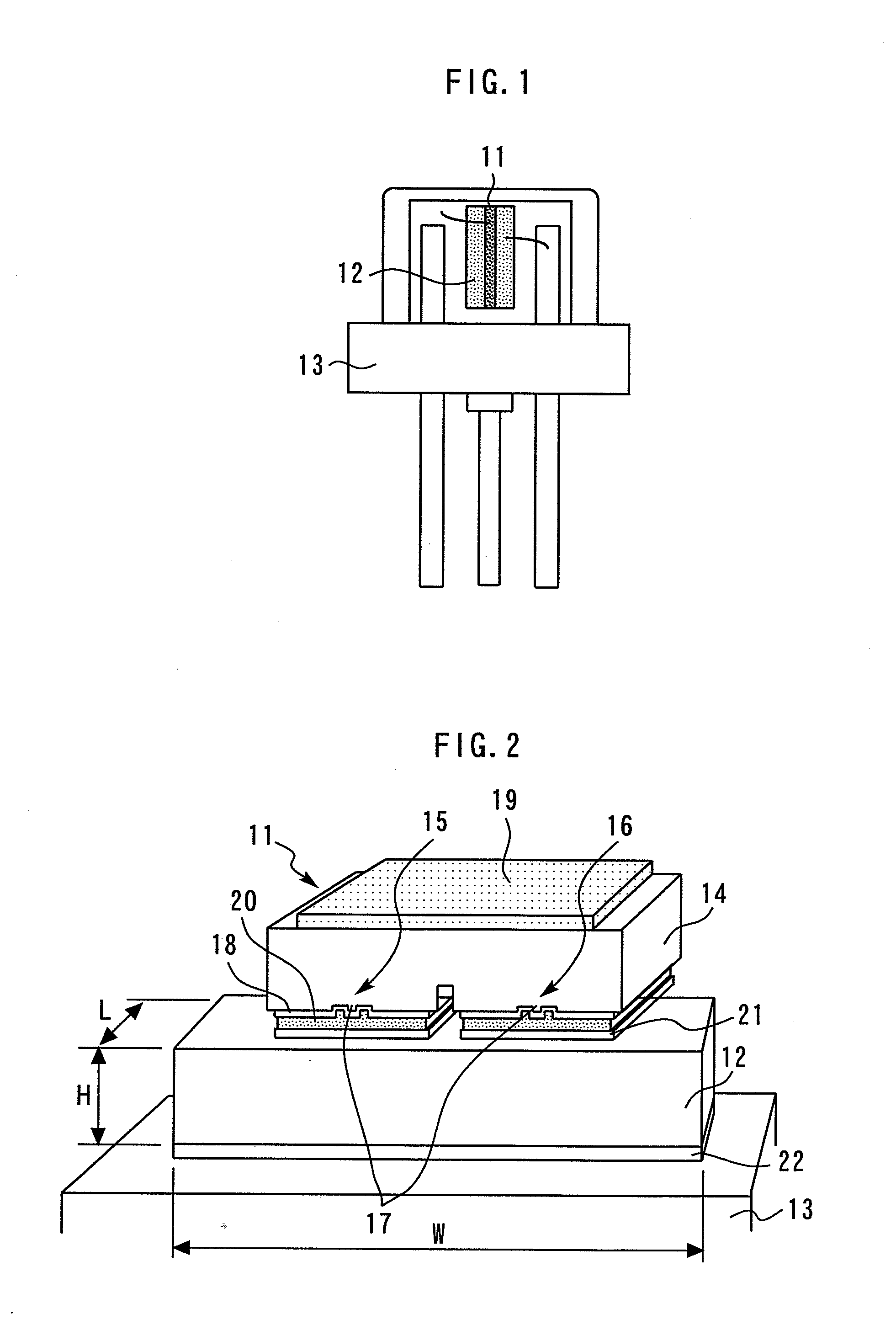
[0030]FIG. 1 is a plan view showing a semiconductor light emitting device according to the first embodiment. The semiconductor light emitting device is a stem package formed by joining a semiconductor laser chip 11 on an AlN sub-mount 12 in a junction-down manner, and joining the AlN sub-mount 12 (sub-mount) to a Cu stem 13 (package). In place of the Cu stem 13, a stem formed of Fe may be used.

[0031]FIG. 2 is a perspective view showing joining portions of the semiconductor laser chip and the sub-mount in the semiconductor light emitting device according to the first embodiment. The semiconductor laser chip 11 is a two-wavelength laser formed by integrating a ridge-type CD laser 15 and a ridge-type DVD laser 16 on a GaAs substrate 14. The ridge portions of the CD laser 15 and the DVD laser 16 are respective light-emitting points 17. A surface electrode 18 and a back-face electrode 19 are formed on the surface and the back-face of the semiconductor laser chip 11, respectively. An Au p...

second embodiment

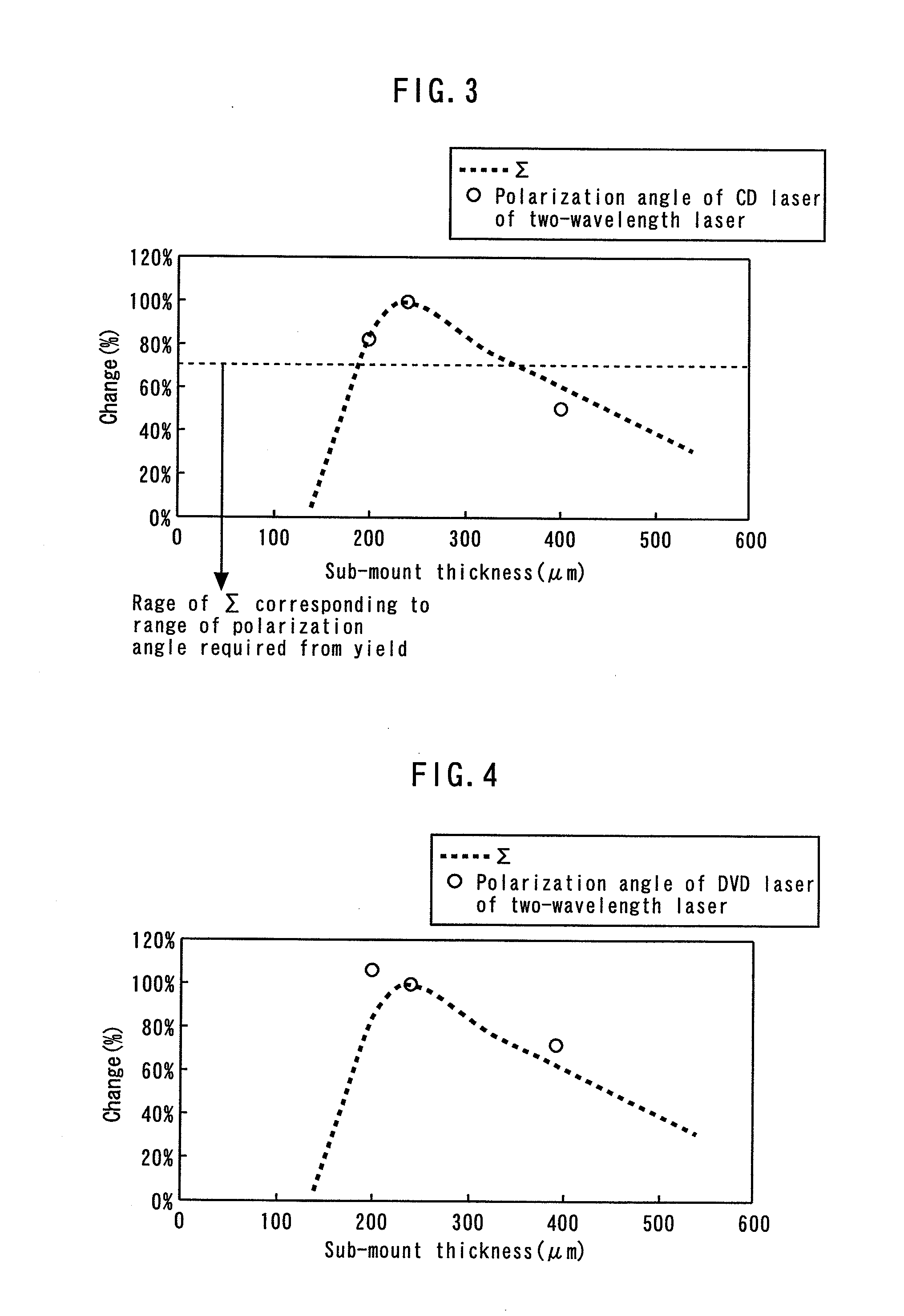
[0044]FIG. 7 is a perspective view showing joining portions of the semiconductor laser chip and the sub-mount in the semiconductor light emitting device according to the second embodiment. The semiconductor laser chip 11 is a single DVD laser 16 formed on a GaAs substrate 14. In the same manner as in the first embodiment, thickness H of the AlN sub-mount 12 is adjusted to reduce the polarizing angle of the laser. A method for the adjustment will be described below in detail.

[0045]First, the results of measuring the polarizing angles of a single DVD laser according to the second embodiment by changing the sub-mount thicknesses H. The size of the semiconductor laser chip 11 is 2200 μm L×180 μm W×100 μm H. However, the thickness of the semiconductor laser chip 11 fluctuates by about ±10 μm due to the fluctuation of manufacturing conditions.

TABLE 5ItemUnitSpec. ASpec. BSpec. CSub-mount length L(μm)217021702170Sub-mount thickness H(μm)200240400Sub-mount width W(μm)600600600Polarization a...

third embodiment

[0049]In the third embodiment, the semiconductor laser chip is a single DVD laser as in the second embodiment. However, although the polarizing angle is reduced by adjusting the sub-mount thickness H in the second embodiment, the polarizing angle is reduced by adjusting the sub-mount width W in the third embodiment. A method for the adjustment will be described below in detail.

[0050]First, the results of measuring the polarizing angles of a single DVD laser according to the third embodiment by changing the sub-mount width W, and measured polarizing angles. The size of the semiconductor laser chip 11 is 2200 μm L×180 μm W×100 μm H. However, the thickness of the semiconductor laser chip fluctuates by about −10 μm due to the fluctuation of manufacturing conditions.

TABLE 7ItemUnitSpec. DSpec. ESub-mount length L(μm)21702170Sub-mount thickness H(μm)240240Sub-mount width W(μm)600800Polarization angle(°)−1.9−0.3(measured)

[0051]Next, based on the value of Σ standardized by the sub-mount wid...


PUM


Abstract

A semiconductor laser chip is joined to an AlN sub-mount in a junction-down manner. The sub-mount is joined to a package. The AlN sub-mount is joined to a stem. The direction perpendicular to the irradiation direction of a laser beam emitted from the semiconductor laser chip is the direction of the width of the sub-mount. The thickness and the width of the AlN sub-mount are determined so that the product of the equivalent stress applied to the center of the surface of the semiconductor laser chip joined to the sub-mount and the stress in the direction of the width of the sub-mount does not exceed 70% of the maximum value of the product obtained by changing the thickness and the width of the AlN sub-mount.

Description

BACKGROUND OF THE INVENTION[0001]1. Field of the Invention[0002]The present invention relates to a semiconductor light emitting device formed by joining a semiconductor laser chip on a sub-mount in a junction-down manner, and more specifically to a semiconductor light emitting device that can reduce the polarizing angle of a laser, and a method for manufacturing such a semiconductor light emitting device.[0003]2. Background Art[0004]GaAs is used as a material of the substrate for a semiconductor laser, and Fe or highly heat-dissipating Cu is used as a material of the package for mounting the semiconductor laser. Here, the coefficient of linear expansion of GaAs is 6 (×10−6 / ° C.), the coefficient of linear expansion of Fe is 11 (×10−6 / ° C.), and the coefficient of linear expansion of Cu is 17 (×10−6 / ° C.). Therefore, when the semiconductor laser having a GaAs substrate is directly adhered to an Fe package with solder or the like, residual stress occurs due to difference in coefficien...

Claims


Application Information

Patent Timeline
IPC IPC(8): H01S5/026H01L33/00H01L23/36H01S5/0231
CPCH01S5/02212H01S5/0224H01S5/02244H01S5/4087H01S5/02476H01S5/4031H01S5/02272H01S5/0231H01S5/0237H01S5/0234
Inventor YAMAGUCHI, TSUTOMUTASHIRO, YOSHIHISAMORI, KENZOSAKAMOTO, HIROONISHIDA, TAKEHIRO
Owner MITSUBISHI ELECTRIC CORP
Why Eureka
Try Eureka