Semiconductor device

a semiconductor memory and device technology, applied in static storage, digital storage, instruments, etc., can solve the problems of volatile semiconductor memory, incompatibility with small circuit size, and risk of reading data incorrectly, so as to reduce the effect of parasitic capacitive coupling, high accuracy, and low cos

Inactive Publication Date: 2012-04-26
LAPIS SEMICON CO LTD
View PDF5 Cites 1 Cited by
  • Summary
  • Abstract
  • Description
  • Claims
  • Application Information

AI Technical Summary

Benefits of technology

[0016]The selector elements are switched on and off to connect different memory cells to the main bit lines at different timings. The fixed potential lines reduce the effect of parasitic capacitive coupling between main bit lines and make it possible to read data with high accuracy.
[0017]The selector elements enable half of the main bit lines in a conventional semiconductor memory to be replaced by fixed potential lines without reducing the number of memory cells. The fixed potential lines can be laid out in the same ways as the main bit lines they replace, in relation to the memory cells, so the replacement does not alter the size of the semiconductor memory. The selector elements themselves take up comparatively little space. The invention is therefore readily applicable to high-density semiconductor memory devices.

Problems solved by technology

In a semiconductor memory, however, since adjacent bit lines are separated by a dielectric material, there is a parasitic capacitance between them, causing the following problem.
Accordingly, there is the risk of reading data incorrectly due to the effect of the parasitic capacitance between the bit lines.
This problem can also occur in volatile semiconductor memory,
This problem can be solved by additionally providing, between each pair of adjacent bit lines, a line that is tied to a fixed potential such as the ground potential, but this solution is incompatible with small circuit size.
The small form factors of recent non-volatile and volatile semiconductor memories make the insertion of such additional lines between the bit lines extremely difficult.

Method used


Image

  • Semiconductor device
  • Semiconductor device
  • Semiconductor device

Examples


Embodiment Construction

[0025]A semiconductor memory embodying the invention will now be described with reference to the attached drawings, in which like elements are indicated by like reference characters.

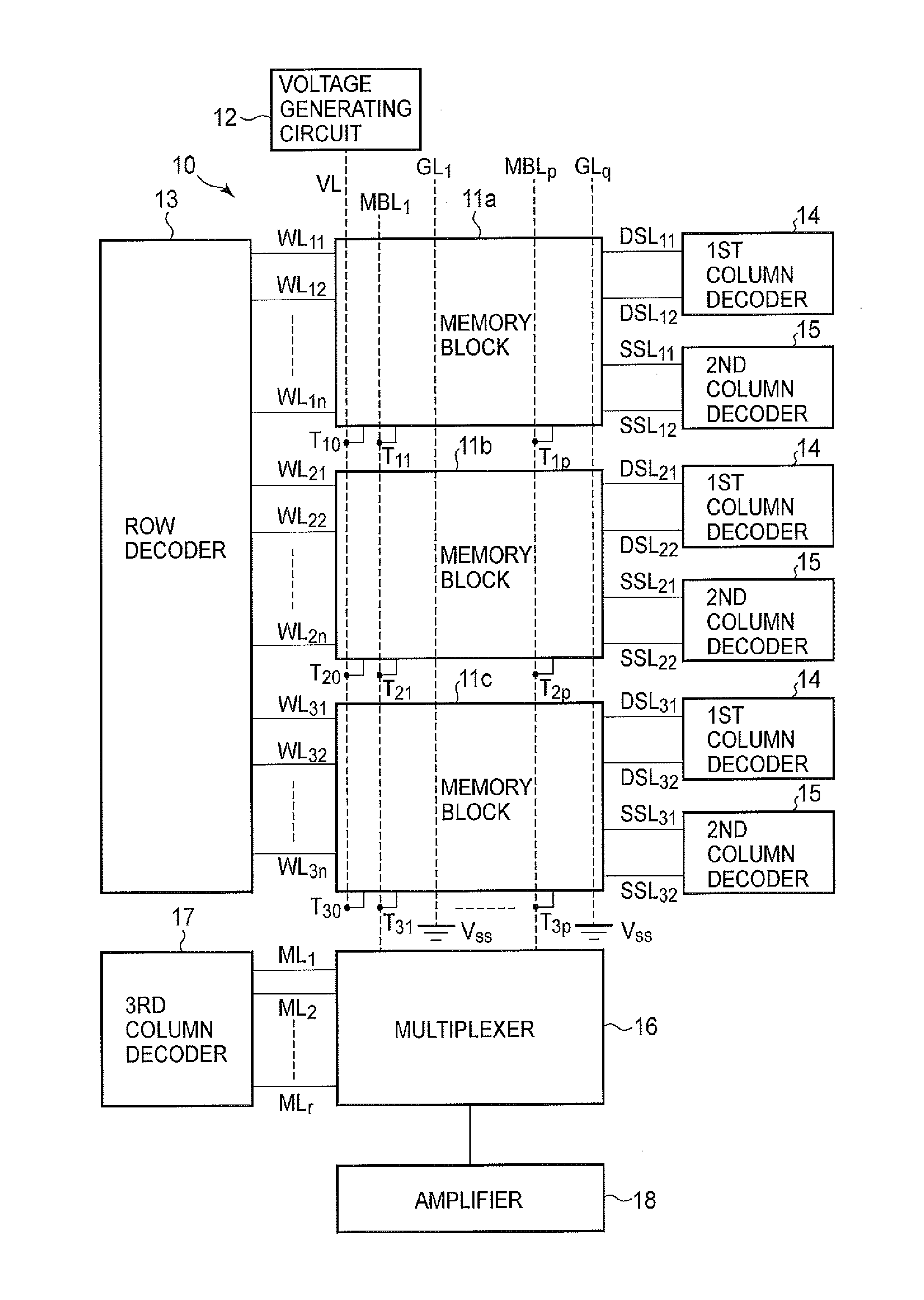
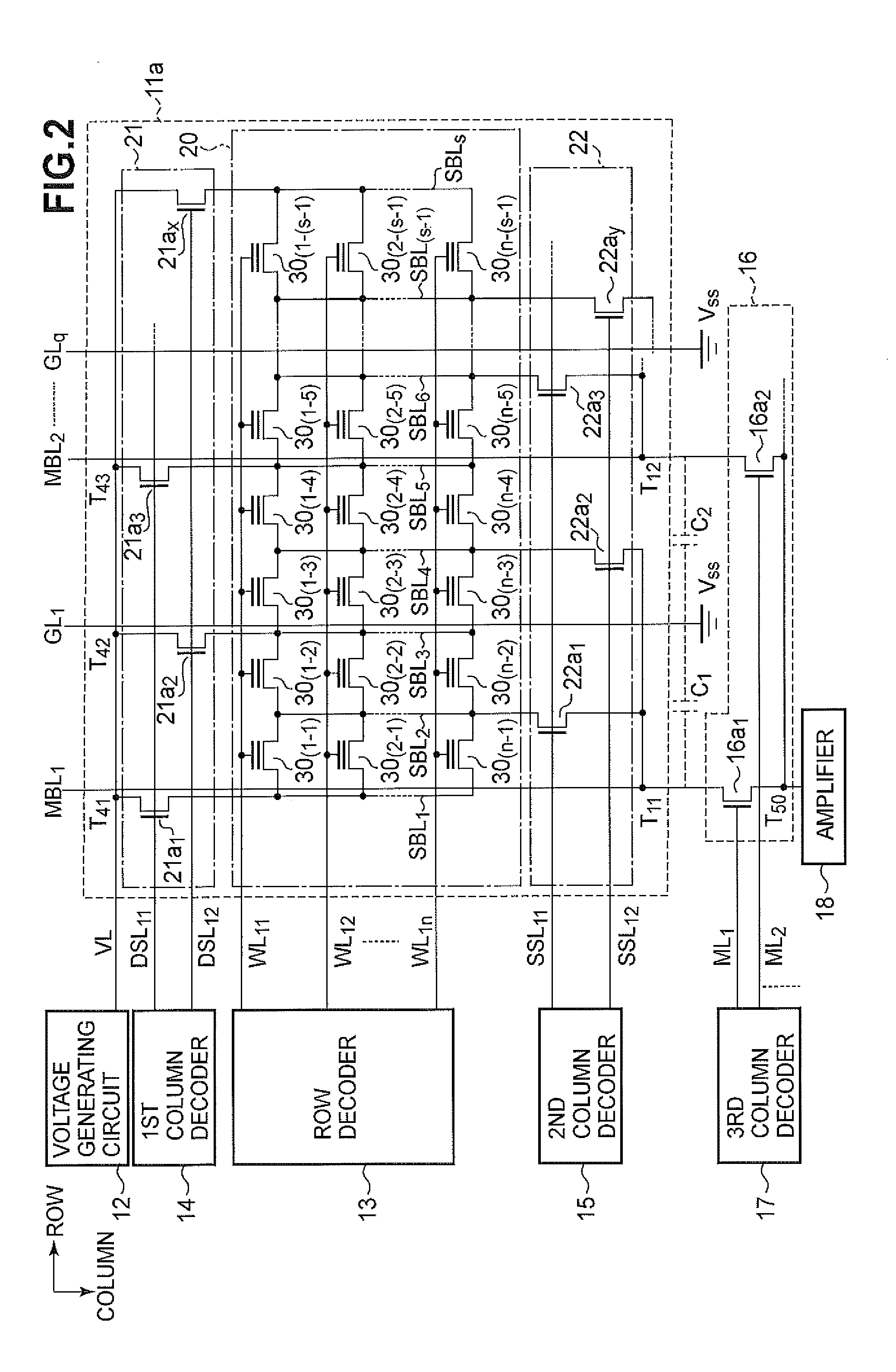
[0026]Referring to the block diagram in FIG. 1, the semiconductor memory 10 includes three memory blocks 11a, 11b, 11c that receive a predetermined voltage from a voltage generating circuit 12. The memory blocks are connected in common to a row decoder 13 and a multiplexer 16, and each memory block is also connected separately to a first column decoder 14 and a second column decoder 15. The multiplexer 16 is connected to a third column decoder 17 and an amplifier 18. The row decoder 13, first column decoders 14, second column decoders 15, and third column decoder 17 function as driving circuits.

[0027]The memory blocks 11a, 11b, 11c are connected to the multiplexer 16 via p main bit lines MBL1, MBL2, . . . , MBLp (where p is a positive integer). Reference characters MBL will be used without subscripts whe...


PUM


Abstract

A semiconductor memory has main bit lines paralleled by fixed potential lines in an alternating arrangement. Each main bit line is switchably connected to two sub-bit lines. The memory cells connected to one of the two sub-bit lines are placed below the main bit line. The memory cells connected to the other one of the two sub-bit lines are placed below an adjacent fixed potential line. The fixed potential lines prevent parasitic capacitive coupling between the main bit lines and thereby speed up read access to the memory cells without taking up extra layout space.

Description

BACKGROUND OF THE INVENTION[0001]1. Field of the Invention[0002]The present invention relates to a semiconductor memory having a plurality of memory cells.[0003]2. Description of the Related Art[0004]Two main types of memory are used to store digital information in electronic devices. One type uses mechanisms such as magnetic or optical disk drives that require physical motion. The other type uses semiconductor memory elements that do not require physical motion. Semiconductor memory can be further classified as volatile, meaning that the stored information is lost when power is switched off, or nonvolatile, meaning that the stored information is retained even while power is off.[0005]In a nonvolatile memory such as an erasable programmable read only memory (EPROM) each memory cell typically has a single charge-storage region. The original or non-programmed state in which no charge is stored in the charge storage region is defined as the ‘1’ state; the written state or programmed st...

Claims


Application Information

Patent Timeline
Patent Type & Authority Applications(United States)
IPC IPC(8): G11C7/10
CPCG11C16/0483G11C16/06
Inventor SHINODA, TATSURU
Owner LAPIS SEMICON CO LTD
Why Eureka
Try Eureka