Transmission circuit and communication device

a technology of transmission circuit and communication device, applied in the field of transmission circuit, can solve the problems of linearity deterioration, poor power efficiency, high linearity, etc., and achieve the effects of wide bandwidth, smooth switching, and rapid detection of output power variation

Inactive Publication Date: 2012-04-26
PANASONIC CORP
View PDF1 Cites 241 Cited by
  • Summary
  • Abstract
  • Description
  • Claims
  • Application Information

AI Technical Summary

Benefits of technology

[0048]As described above, the transmission circuit of the present invention adjusts a timing of switching a voltage to be supplied to the collector terminal of the power amplifier when switching the operation mode, thereby preventing the collector terminal of the power amplifier from being in the no input state. Also, the transmission circuit adjusts a switching timing between the first variable gain amplifier and the second variable gain amplifier, thereby preventing the base terminal of the power amplifier from being in the no input state. Also, when switching the operation mode, the transmission circuit adjusts the switching timing between the first bias circuit and the second bias circuit, thereby preventing the power amplifier from being in the unbiased state. This allows, when switching the operation

Problems solved by technology

However, the conventional quadrature modulation circuit has a characteristic that, when the output power is low, the linearity is high but the power efficiency is poor.
In addition, the conventional polar modulation circuit has a characteristic that t

Method used


Image

  • Transmission circuit and communication device
  • Transmission circuit and communication device
  • Transmission circuit and communication device

Examples


first embodiment

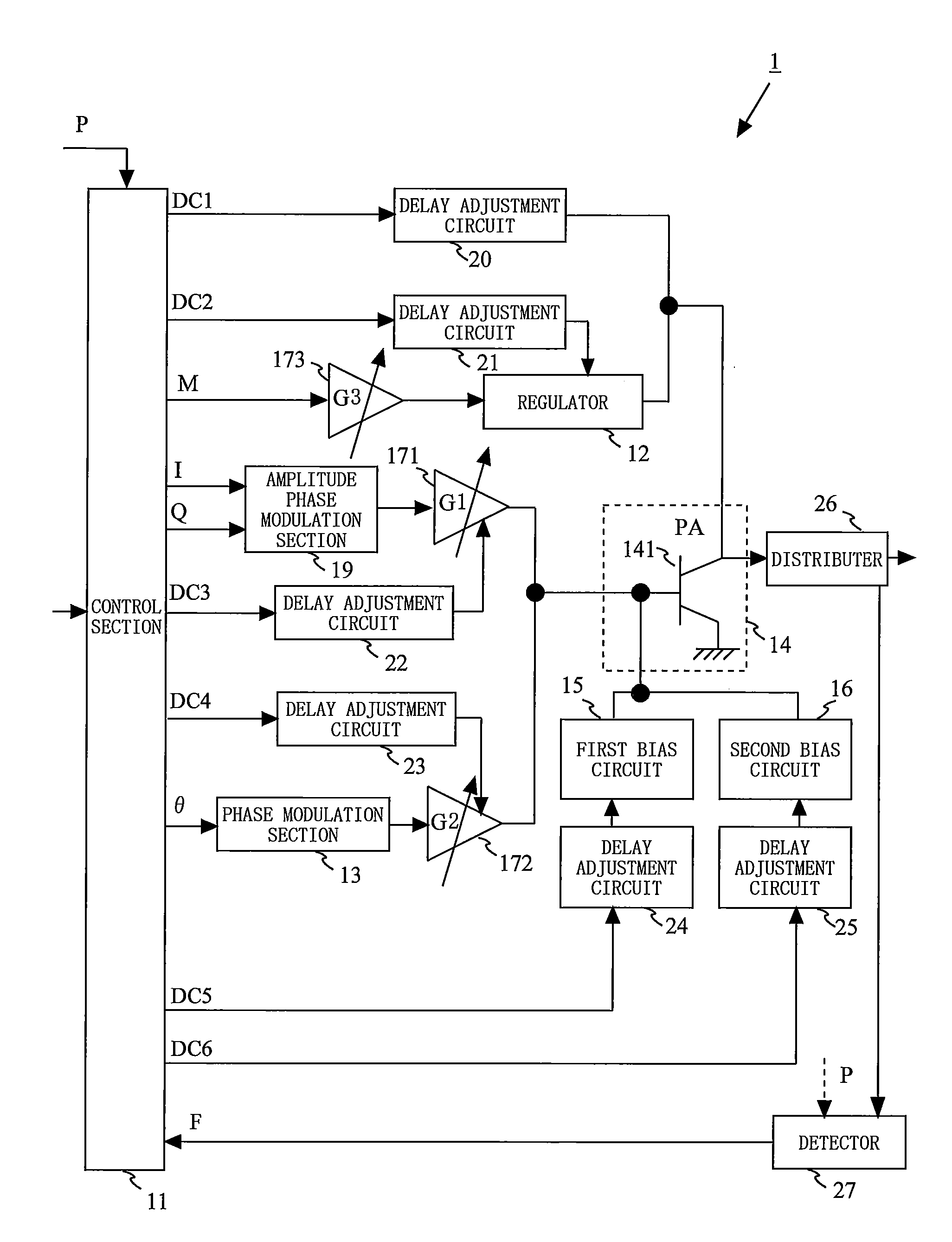
[0083]FIG. 1 is a block diagram showing an example of a configuration of a transmission circuit 1 according to a first embodiment of the present invention. In FIG. 1, the transmission circuit 1 includes a control section 11, a regulator 12, a phase modulation section 13, a power amplifier (PA) 14, a first bias circuit 15, a second bias circuit 16, a first variable gain amplifier 171, a second variable gain amplifier 172, a third variable gain amplifier 173, an amplitude phase modulation section 19, delay adjustment circuits 20, 21, 22, 23, 24, and 25, a distributer 26, and a detector 27. The power amplifier 14 includes an amplifying transistor 141.

[0084]A baseband signal and power information P are inputted to the transmission circuit 1. The power information P is information indicative of the magnitude of output power of the transmission circuit 1, and is, in the W-CDMA system for example, controlled per slot time by a base station.

[0085]The control section 11 controls an operation...

second embodiment

[0166]FIG. 17 is a block diagram showing an example of a configuration of a communication device 200 according to a second embodiment of the present invention. Referring to FIG. 17, the communication device 200 according to the second embodiment includes a transmission circuit 210, a reception circuit 220, an antenna duplexer 230, and an antenna 240. The transmission circuit 210 is any of the transmission circuits of the first embodiment described above. The antenna duplexer 230 transfers a transmission signal, which is outputted from the transmission circuit 210, to the antenna 240, and prevents leakage of the transmission signal to the reception circuit 220. The antenna duplexer 230 also transfers a reception signal, which is inputted thereto from the antenna 240, to the reception circuit 220, and prevents leakage of the reception signal to the transmission circuit 210.

[0167]Therefore, the transmission signal is outputted from the transmission circuit 210 and emitted from the ante...


PUM


Abstract

Provided is a transmission circuit which allows smooth switching of the operation mode when switching the operation mode of the transmission circuit. A power amplifier 14 includes: a first input terminal to which a direct-current voltage or a voltage in accordance with an amplitude signal M is supplied; a second input terminal to which an output signal from a first variable gain amplifier 171 or an output signal from a second variable gain amplifier 172 is inputted; and a third input terminal to which an output signal from a first bias circuit 15 or an output signal from a second bias circuit 16 is inputted. A control section 11 switches the operation mode of the transmission circuit so that at least one of the first input terminal, the second input terminal, and the third input terminal of the power amplifier is prevented from being in a no input state.

Description

TECHNICAL FIELD[0001]The present invention relates to a transmission circuit for use in communication devices such as mobile phones, wireless LAN devices, and the like, and more particularly, a transmission circuit which operates at high precision and high efficiency, and a communication device using the same.BACKGROUND ART[0002]In the advanced information society in recent years, communication devices such as mobile phones, wireless LAN devices, and the like are required to ensure the linearity of a transmission signal over a wide range of power amplification and also operate with low power consumption. In such a communication device, a transmission circuit which outputs a high-precision transmission signal regardless of the bandwidth and operates at high efficiency is employed. A conventional transmission circuit will be described below.[0003]Examples of the conventional transmission circuit include transmission circuits (hereinafter, referred to as a quadrature modulation circuit...

Claims


Application Information

Patent Timeline
IPC IPC(8): H04L27/04H03F3/04
CPCH03F1/0261H03F3/19H03F3/245H03F1/0211H03F2200/336H04B1/406H03F2200/18
Inventor KITAMURA, RYOMIYAZAKI, TAKAHITO
Owner PANASONIC CORP
Why Eureka
Try Eureka