Light-emitting device and electronic apparatus

a technology of light-emitting devices and electronic devices, which is applied in the direction of transistors, optics, instruments, etc., can solve the problems of inhibiting high-precision control of the behavior of light-emitting elements, parasitic capacity between adjacent components, etc., and achieves the effect of reducing the space between the drive transistor and the capacitor element, reducing the parasitic capacity, and suppressing the parasitic capacity

Active Publication Date: 2012-05-03
LUMITEK DISPLAY TECH LTD
View PDF4 Cites 19 Cited by
  • Summary
  • Abstract
  • Description
  • Claims
  • Application Information

AI Technical Summary

Benefits of technology

[0007]An advantage of the invention is to suppress a parasitic capacity influencing on light emission of a light-emitting element.
[0008]According to a first aspect of the invention, a light-emitting device includes a drive transistor for controlling the quantity of current supplied to a light-emitting element, a capacitor element (e.g., a capacitor element C1 shown in FIG. 2 or a capacitor element C2 shown in FIGS. 25 and 26) electrically connected to a gate electrode of the drive transistor, and an electrical continuity portion (e.g., an electrical continuity portion 71, 72, or 73 in each embodiment) for electrically connecting the drive transistor and the light-emitting element, these elements being disposed on a substrate. The electrical continuity portion is disposed on the side opposite to the capacitor element with the drive transistor disposed therebetween. The light-emitting device will be described below with reference to first to third embodiments of the invention.
[0009]In this configuration, the electrical continuity portion is disposed on the side opposite to the capacitor element with the drive transistor provided therebetween, and thus a capacity parasitic to the capacitor element and the electrical continuity portion is decreased, as compared with a configuration in which the electrical continuity portion is disposed in the space between the drive transistor and the capacitor element. Therefore, a variation in potential of one of the capacitor element and the electrical continuity portion has a smaller effect on the potential of the other.
[0010]The capacitor element is typically used for setting or storing the potential of the gate electrode of the drive transistor. For example, the capacitor element (e.g., the capacitor element C1 shown in FIG. 2) is interposed between the gate electrode of the drive transistor and a data line. In this case, the gate electrode of the drive transistor is set to a potential by capacity coupling in the capacitor element according to a variation in potential of the data line. Alternatively, the capacitor element (the capacitor element C2 shown in FIGS. 25 and 26) may be interposed between the gate electrode of the drive transistor and wiring (e.g., a power line) to which a given potential is supplied. In this case, the potential supplied to the gate electrode of the drive transistor is held in the capacitor element.
[0011]The drive transistor preferably includes a semiconductor layer having a channel region formed therein and a gate electrode opposed to the channel region with a gate insulating layer provided therebetween. The capacitor element preferably includes a first electrode (e.g., an electrode E1 shown in FIG. 2) electrically connected to the gate electrode and a second electrode (e.g., an electrode E2 shown in FIG. 2) opposed to the first electrode with the gate insulating layer provided therebetween. The electrical continuity portion is preferably formed on the surface of an insulating layer (e.g., a first insulating layer L1 shown in FIG. 4) covering the gate electrode and the first electrode. In this case, the electrical continuity portion is formed using a layer different from that of the drive transistor and the capacitor element, thereby further decreasing a capacity parasitic between the electrical continuity portion and the capacitor element.
[0012]The first electrode of the capacitor element is more preferably connected to the gate electrode of the drive transistor (e.g., an intermediate conductor 51, 52, or 53 in each embodiment). In this case, the space between the drive transistor and the capacitor element can be decreased, as compared with a configuration in which the first electrode and the gate electrode are formed with a space therebetween.

Problems solved by technology

However, in this case, a capacity is parasitic between adjacent components.
There is thus the problem of inhibiting high-precision control of the behavior of a light-emitting element (emission time and quality of light) due to the capacity parasitic to each component.

Method used


Image

  • Light-emitting device and electronic apparatus
  • Light-emitting device and electronic apparatus
  • Light-emitting device and electronic apparatus

Examples


first embodiment

B-1: First Embodiment

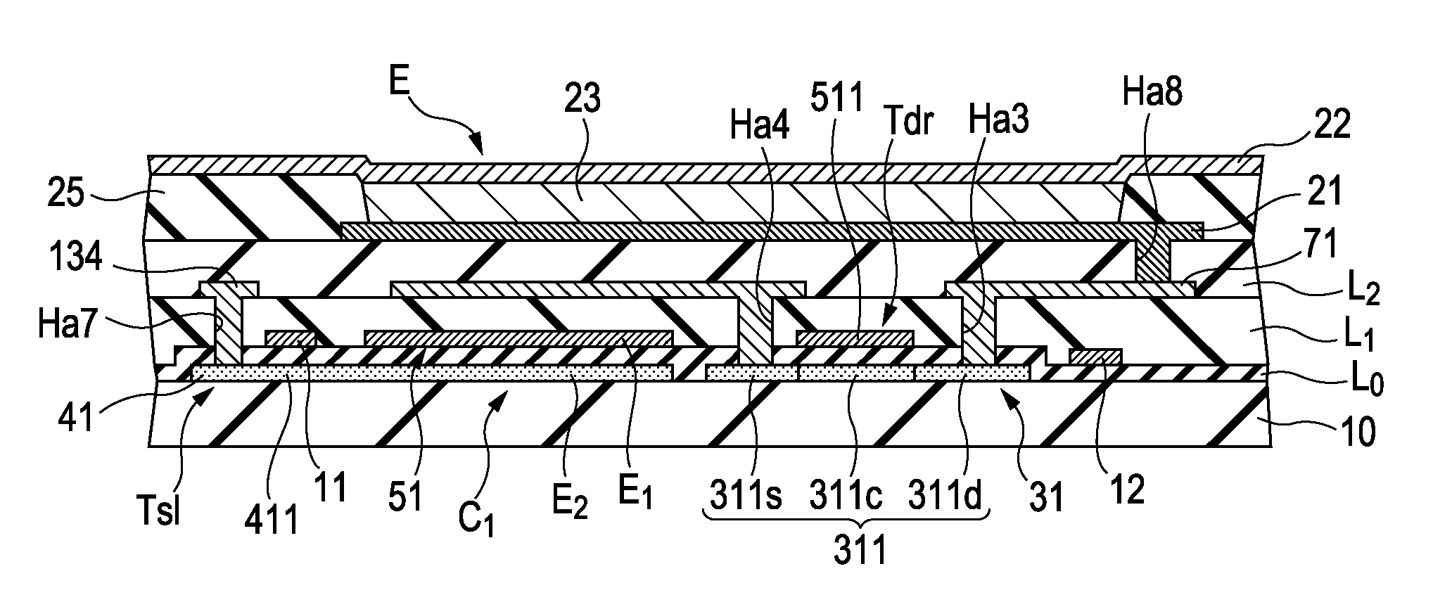
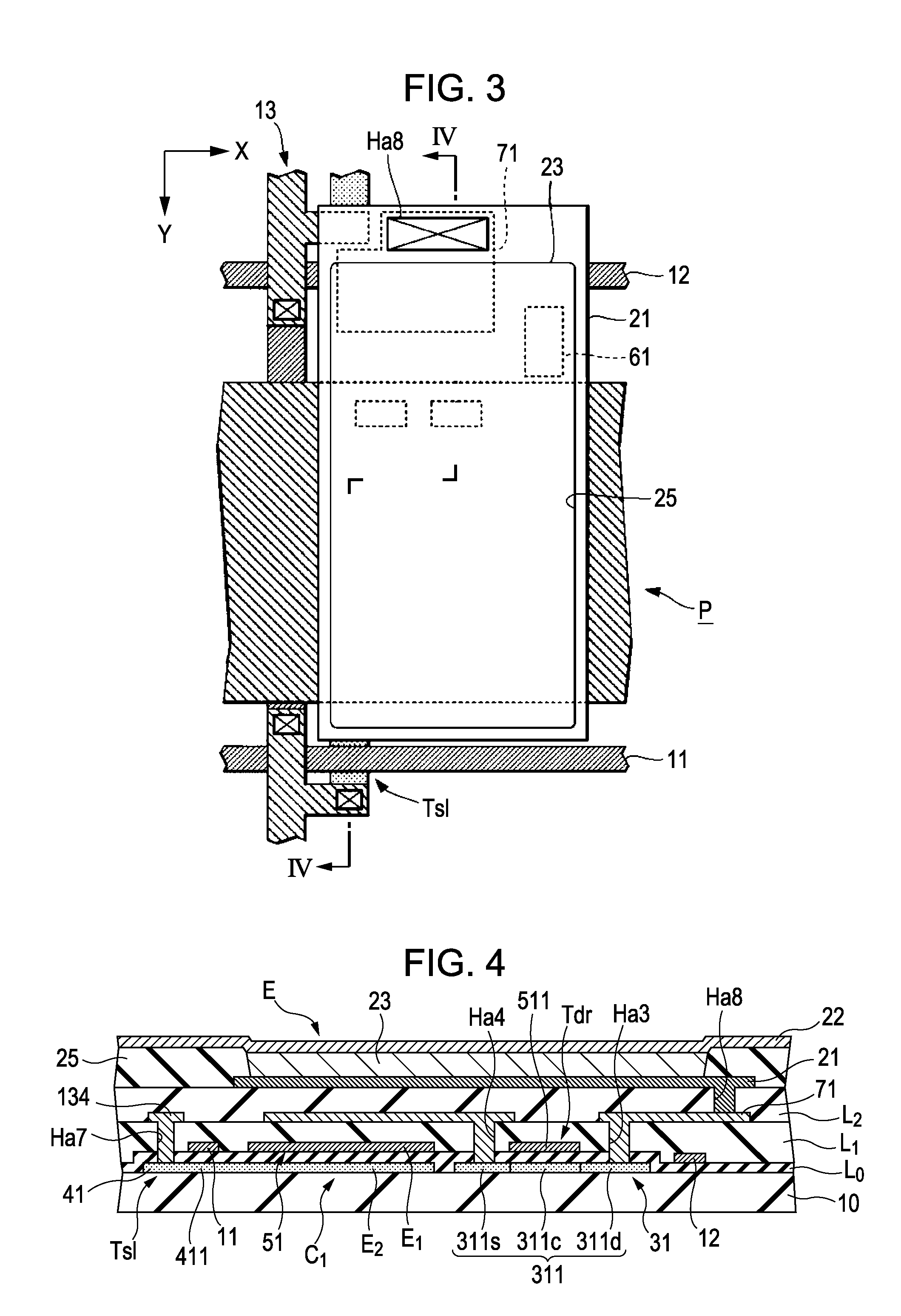
[0063]First, description will be made of the specific structure of the unit element P in a light-emitting device D according to a first embodiment of the invention. FIG. 3 is a plan view showing the configuration of one unit element P, and FIG. 4 is a sectional view taken along line IV-IV in FIG. 3. Although FIG. 3 is a plan view, a component common to that shown in FIG. 4 is hatched in a similar manner to in FIG. 4 in order to facilitate the understanding of each component. This applies to the other plan views referred to below.

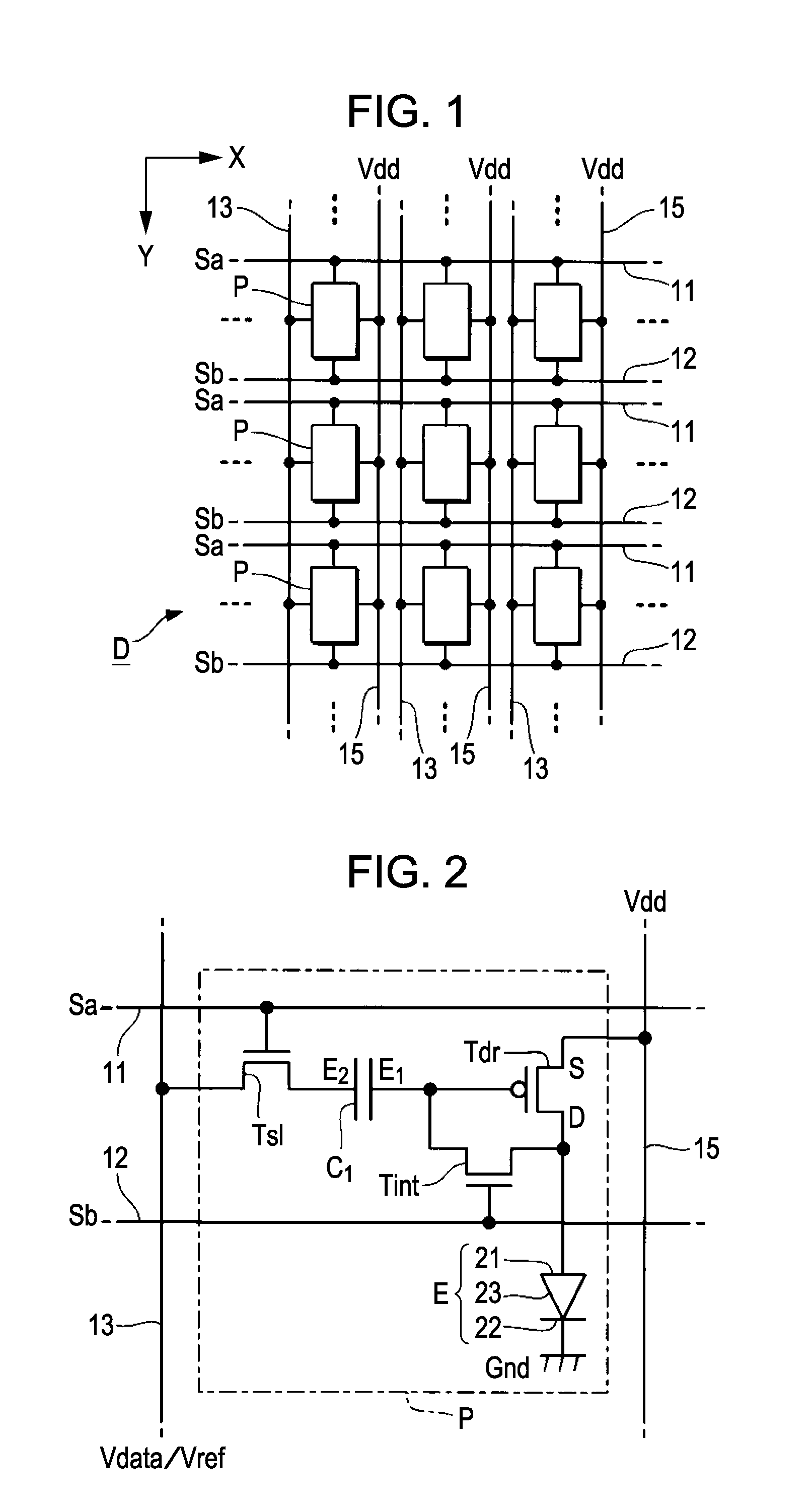
[0064]As shown in FIG. 4, the components such as the drive transistor Tdr and the light-emitting element E shown in FIG. 2 are formed on the surface of a substrate 10. The substrate 10 is a plate-shaped member composed of any one of various insulating materials, such as glass and plastics. The components of the unit element P may be formed on an insulating film (e.g., a film of silicon oxide or silicon nitride) provided as an underlying ...

second embodiment

Modified Example of Second Embodiment

[0124]Next, a modified example of the above-described second embodiment will be described. FIG. 17 is a plan view showing the step (the step shown in FIG. 14) of forming the first insulating layer L1 in this modified example. In the second embodiment, the gate electrode 521 of the drive transistor Tdr extends in the Y direction. However, in the modified example, as shown in FIG. 17, the gate electrode 521 extends in the X direction. In the modified example, the same components as in the second embodiment are denoted by the same reference numerals, and the description thereof is appropriately omitted.

[0125]As shown in FIG. 17, in this embodiment, the intermediate conductor 52 includes a connecting portion 525 extending from the upper left part of the electrode E1 to the negative side in the Y direction and a gate electrode 521 extending from the connecting portion 525 in the X direction and overlapping the semiconductor layer 32. The gate electrod...

third embodiment

B-3: Third Embodiment

[0130]Next, the specific configuration of a unit element P according to a third embodiment of the invention will be described. FIG. 19 is a plan view showing the configuration of a unit element P of this embodiment, and FIGS. 20 to 22 are plan views showing the surface of a substrate 10 in respective steps for forming a unit element P.

[0131]As shown in FIG. 20, a semiconductor layer. 33 and a semiconductor layer 43 are formed on the surface of the substrate 10 using the same layer composed of a semiconductor material. The shape of the semiconductor layer 33 is the same as the semiconductor layer 31 of the first embodiment. The semiconductor layer 43 includes a substantially rectangular electrode E2 constituting the capacitor element C1 and an element part 431 connected to the electrode E2. The element part 431 functions as a semiconductor layer of the selection transistor Tsl and includes a portion 431a extending from the lower right portion of the electrode E2 ...


PUM


Abstract

A light-emitting device includes a drive transistor for controlling the quantity of current supplied to a light-emitting element, a capacitor element electrically connected to a gate electrode of the drive transistor, and an electrical continuity portion for electrically connecting the drive transistor and the light-emitting element, these elements being disposed on a substrate. The electrical continuity portion is disposed on the side opposite to the capacitor element with the drive transistor disposed therebetween.

Description

[0001]This is a Continuation of U.S. patent application Ser. No. 11 / 552,745 filed Oct. 25, 2006. The present application claims priority from Japanese Patent Application No. 2005-345298, filed in the Japanese Patent Office on Nov. 30, 2005, the entire disclosure of which is hereby incorporated by reference in its entirety.BACKGROUND[0002]1. Technical Field[0003]The present invention relates to a structure of a light-emitting device utilizing a luminescent material such as an organic electroluminescent (EL) material or the like.[0004]2. Related Art[0005]An active matrix light-emitting device has been proposed, in which transistors (referred to as “drive transistors” hereinafter) are disposed for respective light-emitting elements, for controlling the quantity of current supplied to each light-emitting element according to the gate potential (refer to, for example, Japanese Unexamined Patent Application Publication No. 2004-119219). A capacitor element is connected to a gate electrode...

Claims


Application Information

Patent Timeline
Patent Type & Authority Applications(United States)
IPC IPC(8): H01L33/16H01L33/36
CPCH01L27/326H01L27/3279H01L33/16H01L29/78645H01L27/3262H01L27/3265H01L27/3276H01L27/1251H01L27/1255H01L27/124H10K59/121H10K59/1315H05B33/26G02F1/136213G02F1/136286G02F1/134336H10K59/131H10K59/123H10K59/1213H10K59/1216
Inventor KUBOTA, TAKEHIKOKANDA, EIJINOZAWA, RYOICHI
Owner LUMITEK DISPLAY TECH LTD
Why Eureka
Try Eureka