Photoelectric conversion device

a conversion device and photoelectric technology, applied in the direction of semiconductor devices, electrical devices, nanotechnology, etc., can solve the problem of the theoretical limit of the photoelectric conversion efficiency of the mono-junction solar cell, which remains at about 30%, and achieve the effect of reducing the energy difference between the quantum levels of adjacent quantum structure portions, easy transfer, and easy transfer

Inactive Publication Date: 2012-05-10
TOYOTA JIDOSHA KK
View PDF4 Cites 11 Cited by
  • Summary
  • Abstract
  • Description
  • Claims
  • Application Information

AI Technical Summary

Benefits of technology

[0032]According to the present invention, since the relations Cp1<Cp2 and / or Cn1<Cn2 are satisfied, it is possible to make the band of the i-layer gently-inclined. By making the band of the i-layer gently-inclined, the energy difference between the quantum levels of the adjacent quantum structure portions can be reduced. Therefore, with the present invention, the carrier in the quantum structure portion can be easily transferred by tunneling conduction. By enabling the carrier to be easily transferred, it becomes possible to improve the photoelectric conversion efficiency. Therefore, according to the present invention, it is possible to provide a photoelectric conversion device which is capable of improving the photoelectric conversion efficiency.
[0033]Further, in the present invention, by containing the p-type impurity in the end portion on the n-layer side of the i-layer, it is possible to make gentle the band inclination in the end portion on the n-layer side of the i-layer, where increase in the energy difference between the quantum levels of the adjacent quantum structure portions tends to occur. As a result, it becomes possible to reduce the energy difference between the quantum levels of the quantum structure portion existing in the end portion on the n-layer side of the i-layer, and the quantum level of the quantum structure portion adjacent to the above quantum structure portion; and therefore, a number of electrons can be transferred to the quantum structure portion existing in the end portion on the n-layer side of the i-layer, by tunneling conduction.
[0034]In the present invention, by controlling Cp1 and the concentration of the n-type impurity in the n-layer so that the electron can be transferred to the n-layer from the quantum structure portion contained in the end portion on the n-layer side of the i-layer by tunneling conduction, the electrons existing in the ground quantum level of the quantum structure portion can be easily transferred to the n-layer.
[0035]Also, in the present invention, by setting the energy level at the lower end of the conduction band of the end face on the second electrode side of the n-layer at or below the ground level of the quantum structure portion contained in the end portion on the n-layer side of the i-layer, the electron existing in the quantum structure portion can be easily transferred to the n-layer by tunneling conduction.
[0036]In the present invention, by forming the triangular potential having the quantum level in the conduction band of the n-layer, it becomes possible to transfer the electron to the n-layer through the quantum level of the triangular potential, thereby enabling easily improving the photoelectric conversion efficiency.
[0037]In the present invention, by making the quantum level formed in the conduction band of the n-layer approximately equal to the energy level at the lower end of the conduction band of the end face on the second electrode side of the n+-layer, the photoelectric conversion efficiency can be easily improved.

Problems solved by technology

However, the theoretical limit of the photoelectric conversion efficiency of the mono-junction solar cell (hereinafter, referred to as a “theoretical efficiency limit”.) remains at about 30%; therefore, new methods for further improving the theoretical efficiency limit have been studied.

Method used


Image

  • Photoelectric conversion device
  • Photoelectric conversion device
  • Photoelectric conversion device

Examples


first embodiment

1. A First Embodiment

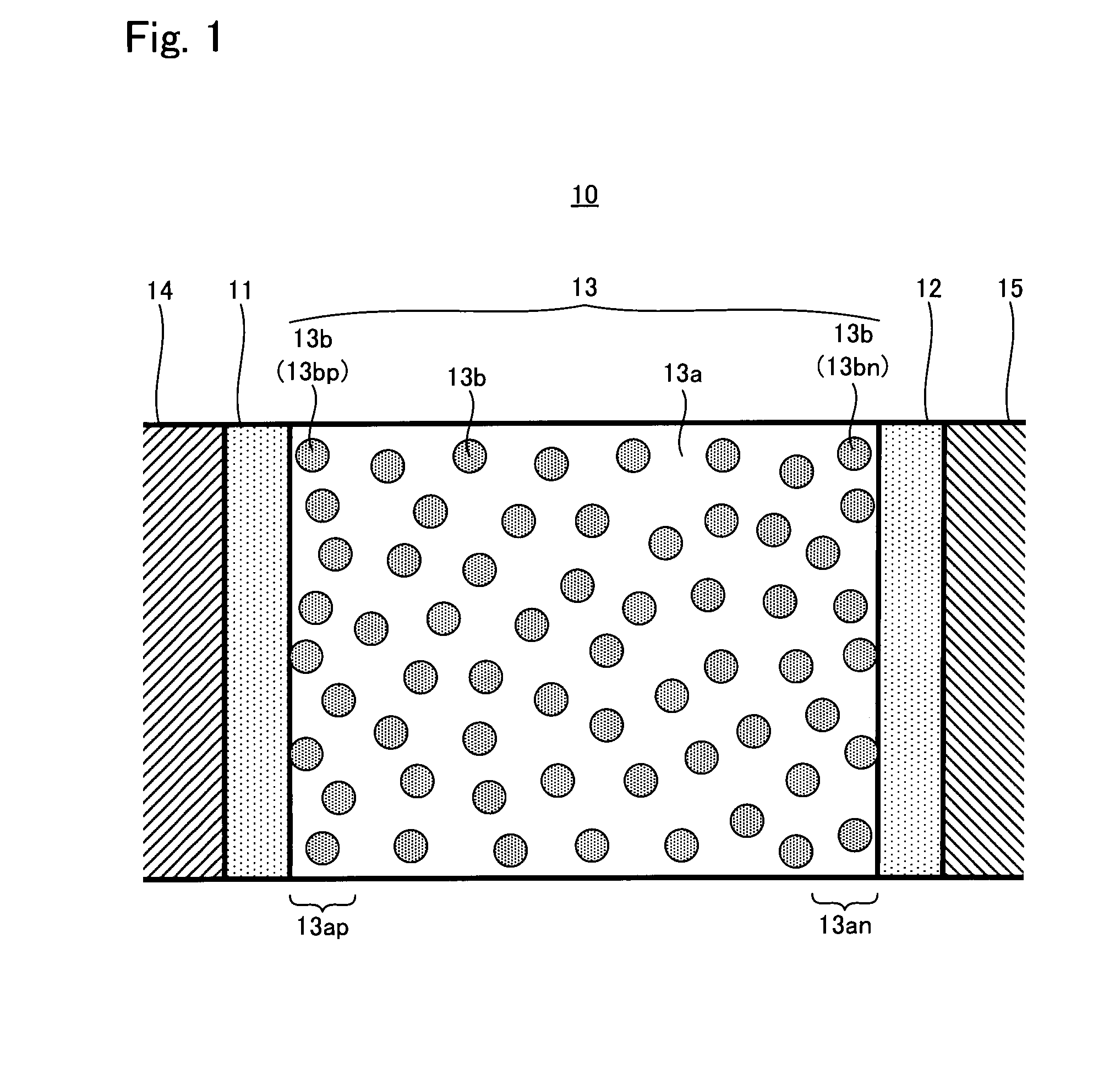
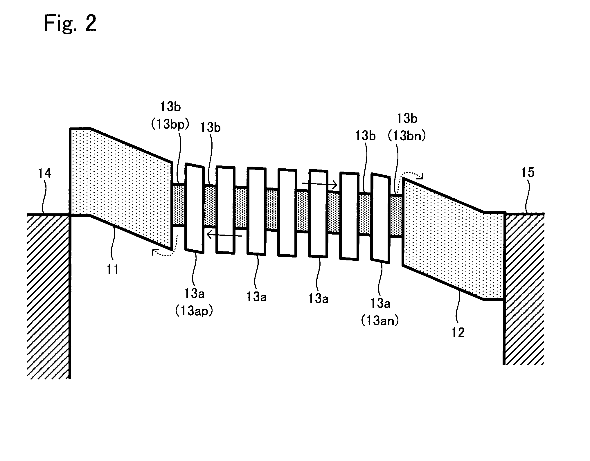
[0103]FIG. 1 is a cross-sectional view illustrating a solar cell 10 in accordance with a first embodiment. Some of the reference numerals are omitted in FIG. 1. As shown in FIG. 1, the solar cell 10 comprises: a p-layer 11; an n-layer 12; an i-layer 13 disposed between the p-layer 11 and the n-layer 12; a first electrode 14 connected to the p-layer 11; and a second electrode connected to the n-layer 12. The i-layer 13 comprises a wall layer 13a and quantum dots 13b, 13b, . . . , (sometimes simply referred to as a “quantum dot 13b”, hereinafter) disposed in the wall layer 13a. The wall layer 13a is constituted by a first semiconductor; and the quantum dots 13b, 13b, . . . are constituted by a second semiconductor having a band gap narrower than that of the first semiconductor. In the solar cell 10, a spacing among the quantum dots 13b, 13b, . . . is configured to permit a carrier to be transferred by tunneling conduction. An n-type impurity is contained in the wa...

second embodiment

2. A Second Embodiment

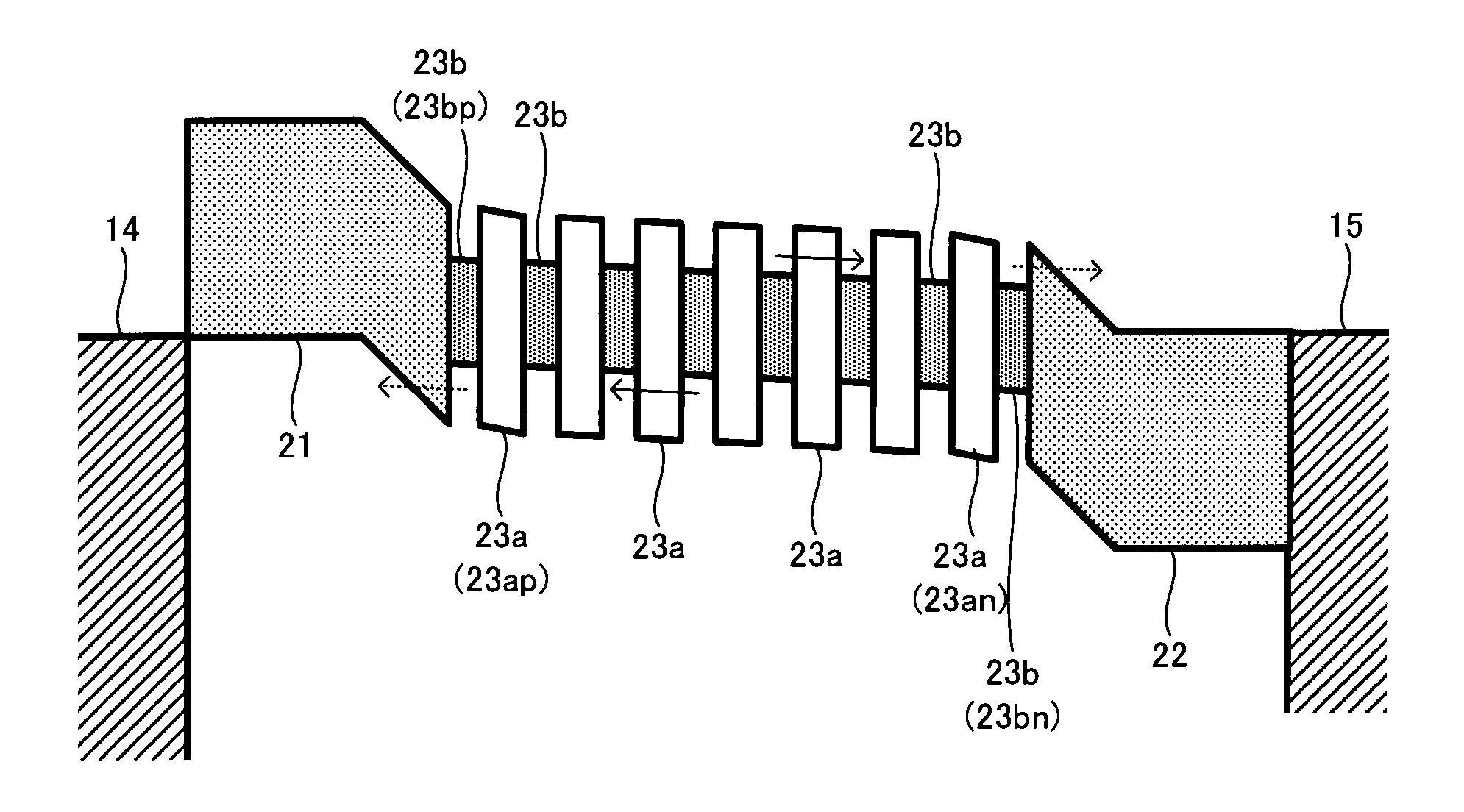
[0115]FIG. 3 is a cross-sectional view illustrating a solar cell 20 in accordance with a second embodiment. Some of the reference numerals are omitted in FIG. 3. In FIG. 3, to the elements having the same structure as those in the solar cell 10, the same reference numerals as those used in FIGS. 1 and 2 are given, and the explanations thereof are adequately omitted.

[0116]As shown in FIG. 3, the solar cell 20 comprises: a p-layer 21; an n-layer 22; an i-layer 23 disposed between the p-layer 21 and the n-layer 22; a first electrode 14 connected to the p-layer 21; and a second electrode 15 connected to the n-layer 22. A concentration of a hole contained in the p-layer 21 is higher than that of the hole contained in the p-layer 11 of the solar cell 10; and a concentration of an electron contained in the n-layer 22 is higher than that of the electron contained in the n-layer 12 of the solar cell 10. The i-layer 23 comprises a wall layer 23a and quantum dots 23b, 23b...

third embodiment

3. A Third Embodiment

[0123]FIG. 5 is a cross-sectional view illustrating a solar cell 30 in accordance with a third embodiment. Some of the reference numerals are omitted in FIG. 5. In FIG. 5, to the elements having the same structure as those in the solar cell 20, the same reference numerals as those used in FIGS. 3 and 4 are given, and the explanations thereof are adequately omitted.

[0124]As shown in FIG. 5, the solar cell 30 comprises: a p-layer 21; an n-layer 22; an i-layer 31 disposed between the p-layer 21 and the n-layer 22; a first electrode 14 connected to the p-layer 21; and a second electrode 15 connected to the n-layer 22. The i-layer 31 is configured in a manner laminating a wall layer 31a; a barrier 31b; and a layer 31e comprising a wet layer 31c and quantum dots 31d, 31d, . . . , (sometimes simply referred to as a “quantum dot 31d”, hereinafter). The wall layers 31a, 31a, . . . , (sometimes simply referred to as a “wall layer 31a”, hereinafter) are constituted by a fi...


PUM


Abstract

A main object of the present invention is to provide a photoelectric conversion device which is capable of improving the photoelectric conversion efficiency. The invention comprises: a p-layer; an n-layer; an i-layer disposed between the p-layer and the n-layer; a first electrode connected to the p-layer; and a second electrode connected to the n-layer, wherein the i-layer comprises a wall layer constituted by a first semiconductor, and a quantum structure portion constituted by a second semiconductor disposed in the wall layer; a band gap of the first semiconductor is wider than that of the second semiconductor; when a concentration of the n-type impurity that may be contained in the middle of the i-layer in a thickness direction thereof is defined as Cn1, a concentration of the n-type impurity that may be contained in the region on the p-layer side of the i-layer is defined as Cn2, a concentration of the p-type impurity that may be contained in the middle of the i-layer in a thickness direction thereof is defined as Cp1, and a concentration of the p-type impurity that may be contained in the region on the n-layer side of the i-layer is defined as Cp2, the relations Cn1<Cn2 and/or Cp1<Cp2 are satisfied.

Description

TECHNICAL FIELD[0001]The present invention relates to a photoelectric conversion device; and particularly relates to a photoelectric conversion device employing the quantum structure.BACKGROUND ART[0002]A Solar cell has advantages that the amount of carbon dioxide emitted per power generation is small and that no fuels for power generation is required. Thus, studies on various types of solar cells have been actively developed. Currently, among the solar cells in practical use, a mono-junction solar cell having a set of p-n junction and using single-crystal silicon or polycrystal silicon has become mainstream. However, the theoretical limit of the photoelectric conversion efficiency of the mono-junction solar cell (hereinafter, referred to as a “theoretical efficiency limit”.) remains at about 30%; therefore, new methods for further improving the theoretical efficiency limit have been studied.[0003]One of the new methods which have been studied so far is a solar cell employing a quan...

Claims


Application Information

Patent Timeline
Patent Type & Authority Applications(United States)
IPC IPC(8): H01L31/06H01L31/02H01L31/075
CPCH01L31/035218H01L31/075Y10S977/948Y10S977/932Y02E10/548
Inventor SUTO, HIROYUKI
Owner TOYOTA JIDOSHA KK
Why Eureka
Try Eureka