Method of depositing dielectric films using microwave plasma

a dielectric film and microwave plasma technology, applied in the direction of basic electric elements, semiconductor/solid-state device manufacturing, electric apparatus, etc., can solve the problems of phenyl terminating sams only 50% of the leakage performance of sin capping layer,/sicn/sico materials are expected to fail,

Active Publication Date: 2012-05-10
TOKYO ELECTRON LTD
View PDF2 Cites 12 Cited by
  • Summary
  • Abstract
  • Description
  • Claims
  • Application Information

AI Technical Summary

Benefits of technology

[0006]Embodiments of the invention describe a method for forming dielectric films using a microwave plasma source, for example a microwave plasma source containing a

Problems solved by technology

Current thickness and dielectric constant scaling remain a difficult challenge for future copper (Cu) capping/etch stop technologies and there are tradeoffs between density, which improves barrier properties, and dielectric constant, which increases with density.
Difficult challenges include identifying materials with good adhesion to the low-dielectric constant (low-k) interlayer dielectric (ILD) and Cu, Cu out diffusion and H2O2/O2 in diffusion prevention, electromigration and leakage, and compatibility with Cu interconnect processing such as ILD etch, photoresist ashing, etc.
The scaling of current low-k SiCN

Method used


Image

  • Method of depositing dielectric films using microwave plasma
  • Method of depositing dielectric films using microwave plasma
  • Method of depositing dielectric films using microwave plasma

Examples


Embodiment Construction

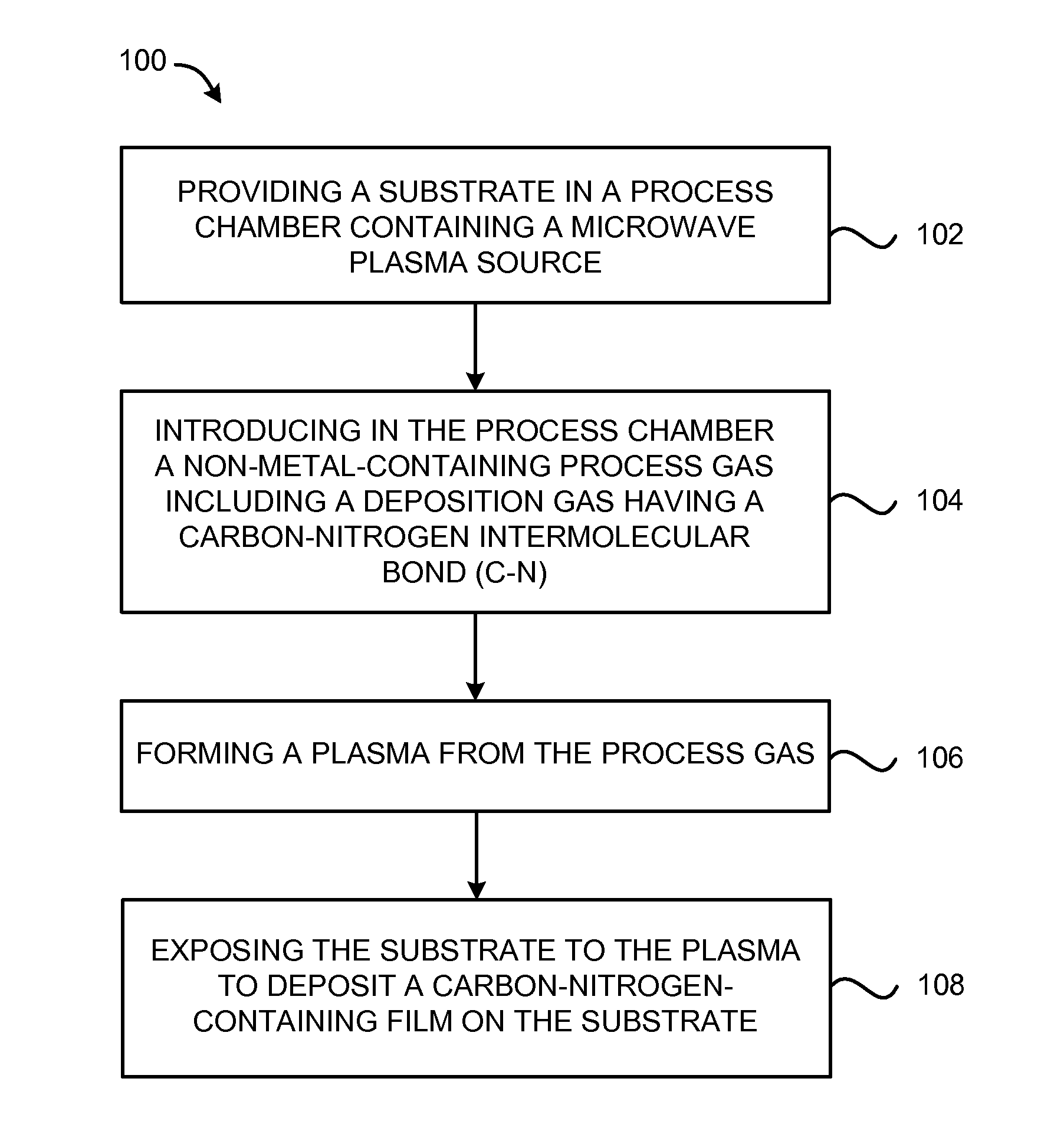
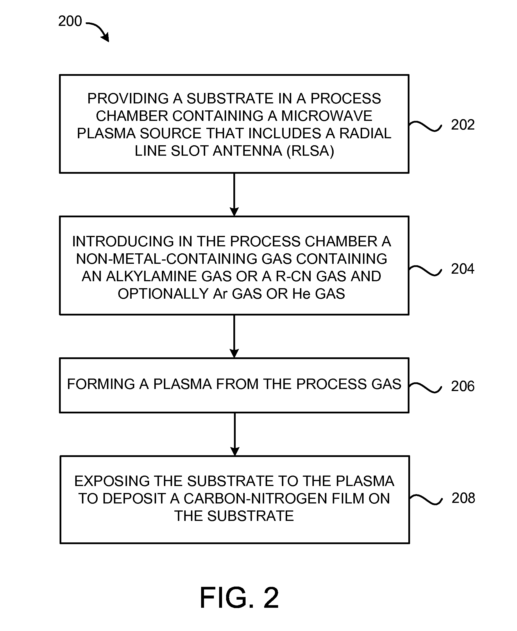
[0021]Methods for depositing dielectric films, including low-k dielectric films, on a substrate using a microwave plasma source are described in various embodiments. The low-k dielectric films have a dielectric constant lower than that of SiO2 (k˜3.9), lower than 3.5, lower than 3, lower than 2.5, or even lower than 2. One skilled in the relevant art will recognize that the various embodiments may be practiced without one or more of the specific details, or with other replacement and / or additional methods, materials, or components. In other instances, well-known structures, materials, or operations are not shown or described in detail to avoid obscuring aspects of various embodiments of the invention. Similarly, for purposes of explanation, specific numbers, materials, and configurations are set forth in order to provide a thorough understanding of the invention. Furthermore, it is understood that the various embodiments shown in the figures are illustrative representations and are ...


PUM


Abstract

Embodiments of the invention describe a method for forming dielectric films for semiconductor devices. The method includes providing a substrate in a process chamber containing a microwave plasma source, introducing into the process chamber a non-metal-containing process gas including a deposition gas having a carbon-nitrogen intermolecular bond, forming a plasma from the process gas, and exposing the substrate to the plasma to deposit carbon-nitrogen-containing film on the substrate. In some embodiments, the carbon-nitrogen-containing film can include a CN film, a CNO film, a Si-doped CN film, or a Si-doped CNO film.

Description

CROSS-REFERENCE TO RELATED APPLICATIONS[0001]This application is related to and claims priority to U.S. Provisional application Ser. No. 61 / 410,155 (Ref. no. RLSA-003Pro) filed on Nov. 4, 2010, the entire contents of which are herein incorporated by reference.FIELD OF THE INVENTION[0002]The present invention generally relates to depositing dielectric films on a substrate using a microwave plasma source.BACKGROUND OF THE INVENTION[0003]Current thickness and dielectric constant scaling remain a difficult challenge for future copper (Cu) capping / etch stop technologies and there are tradeoffs between density, which improves barrier properties, and dielectric constant, which increases with density. Difficult challenges include identifying materials with good adhesion to the low-dielectric constant (low-k) interlayer dielectric (ILD) and Cu, Cu out diffusion and H2O2 / O2 in diffusion prevention, electromigration and leakage, and compatibility with Cu interconnect processing such as ILD etc...

Claims


Application Information

Patent Timeline
IPC IPC(8): H01L21/314
CPCH01L21/02118H01L21/02126H01L21/02274H01L21/02211H01L21/02167
Inventor TAKABA, HIROYUKI
Owner TOKYO ELECTRON LTD
Why Eureka
Try Eureka