Electro-optic device and projection-type display apparatus

a technology of optical devices and projection-type displays, applied in non-linear optics, instruments, optics, etc., can solve the problems of significant thermal stress, decrease in the reflectance decrease in the smooth surface of the pixel electrode, so as to prevent a defect such as hillock

Active Publication Date: 2012-05-17
SEIKO EPSON CORP
View PDF4 Cites 39 Cited by
  • Summary
  • Abstract
  • Description
  • Claims
  • Application Information

AI Technical Summary

Benefits of technology

[0007]An advantage of some aspects of the invention is to provide an electro-optic device capable of preventing a defect such as hillock caused by thermal stress from occurring on the surface of the pixel electrode, and a projection-type display apparatus using the electro-optic device.

Problems solved by technology

However, after the insulating film is formed on the upper layer side of the pixel electrode after forming the reflective pixel electrode, significant thermal stress occurs on the pixel electrode due to heat generated when forming the insulating film, there is a problem in that the thermal stress may cause a defect, such as hillock on the surface of the pixel electrode.
As a result, a defect such as hillock occurs on the surface of the pixel electrode by thermal stress, smoothness of the surface of the pixel electrode decreases, and the reflectance of the pixel electrode decreases.
Since the aluminum film (thermal expansion coefficient=23.1×10⁻⁶ / ° C.) has a great difference in thermal expansion coefficient from the non-doped silicon oxide film (thermal expansion coefficient=0.5×10⁻⁶ / ° C.) or the like, significant thermal stress easily occurs, and a defect such as hillock easily occurs.
According to the configuration, since it is not necessary to perform a rubbing process differently from an organic alignment film, an increase in costs caused by the rubbing process or a difference in alignment characteristic does not occur.

Method used


Image

  • Electro-optic device and projection-type display apparatus
  • Electro-optic device and projection-type display apparatus
  • Electro-optic device and projection-type display apparatus

Examples


embodiment 1

Overall Configuration

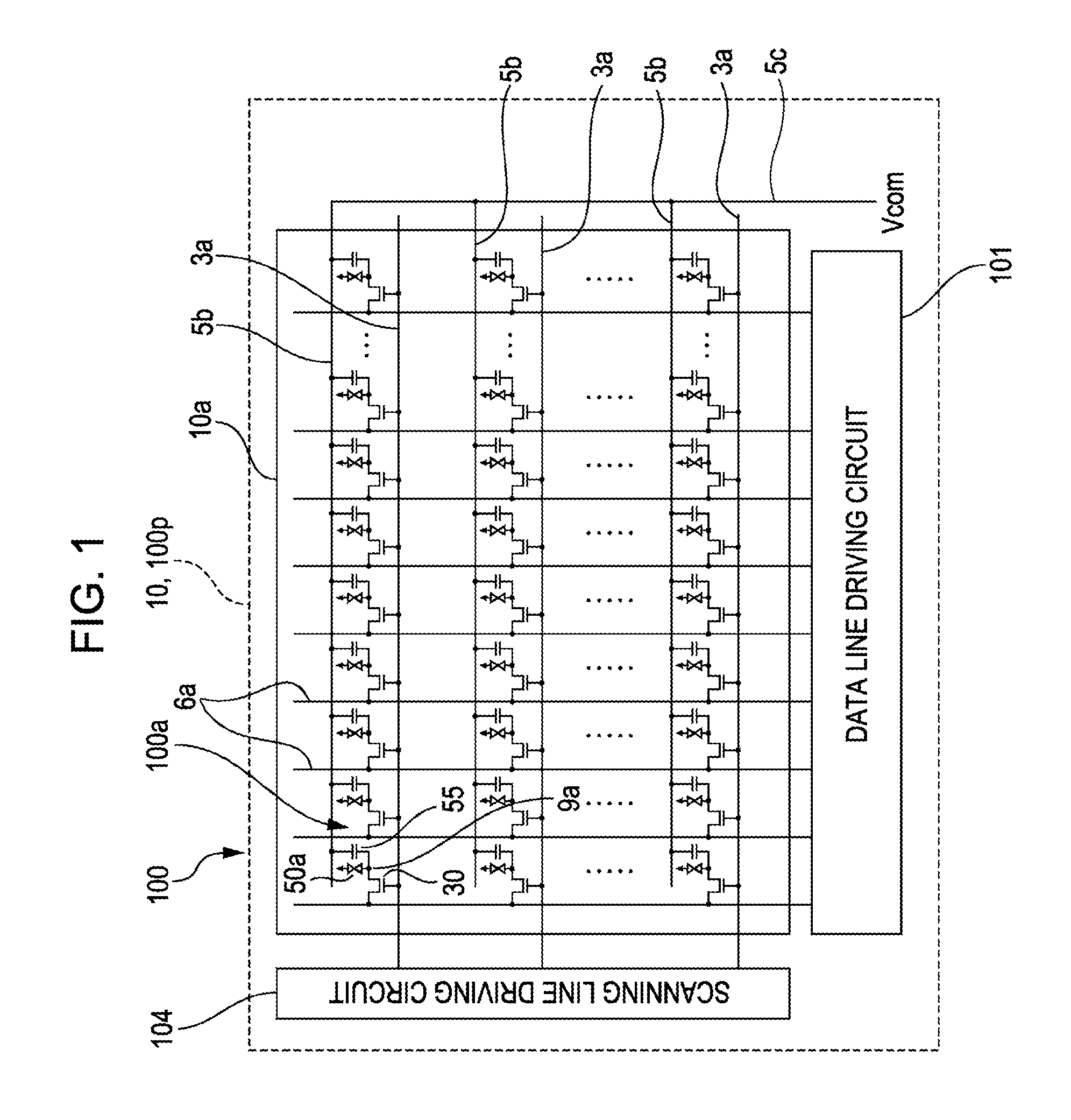
[0033]FIG. 1 is a block diagram illustrating an electrical configuration of an electro-optic device according to the invention. In FIG. 1, an electro-optic device 100 of the embodiment is a reflection-type liquid crystal device, and has a reflection-type liquid crystal panel 100p of a TN (Twisted Nematic) mode or a VA (Vertical Alignment) mode. The liquid crystal panel 100p is provided with a pixel area 10a (image display area) in which a plurality of pixels 100a are arranged in matrix at the center area thereof. In the liquid crystal panel 100p, in an element substrate 10 (see FIG. 2A and FIG. 2B) to be described later, a plurality of data lines 6a and a plurality of scanning lines 3a are longitudinally and transversely arranged in the pixel area 10a, and the pixels 100a are provided at positions corresponding to the intersections thereof. Each of the pixels 100a is provided with a pixel transistor 30 formed of an electric field effect transistor, and a pixel e...

embodiment

Main Effect of Embodiment

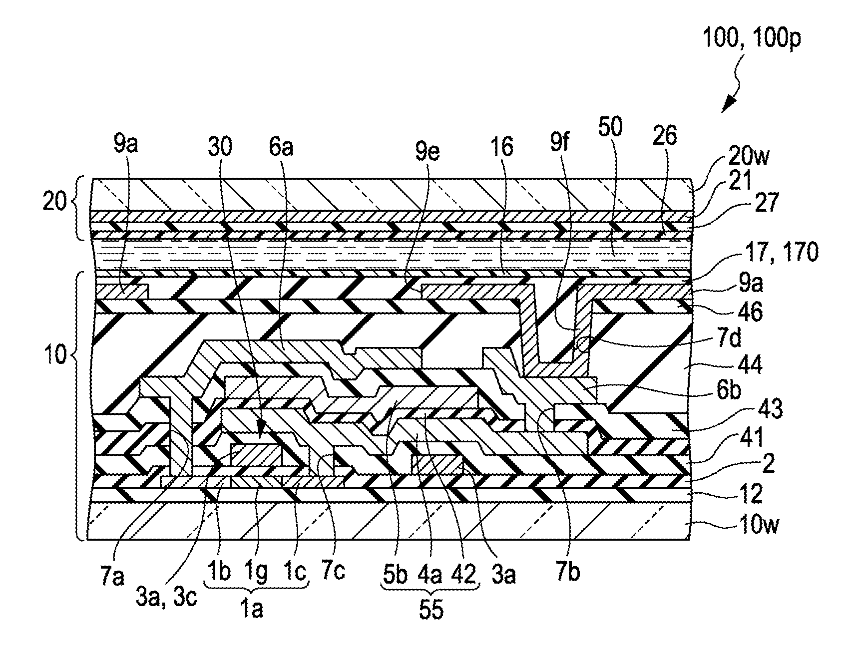
[0069]As described above, in the electro-optic device 100 of the embodiment, the stress relieving film 46 is interposed between the third interlayer insulating film 44 and the pixel electrode 9a, and the stress relieving film 46 has a thermal expansion coefficient different from that of the third interlayer insulating film 44, comes in contact with the third interlayer insulating film 44, has a thermal expansion coefficient different from that of the pixel electrode 9a, and comes in contact with the pixel electrode 9a. For this reason, when the planarized insulating film 17 (insulating film) is formed and even when the thermal stress caused by the difference between the thermal expansion coefficient of the third interlayer insulating film 44 and the thermal expansion coefficient of the pixel electrode 9a occurs in the pixel electrode 9a, it is possible to reduce the occurrence of the thermal stress as compared with the case where the third interlayer insulat...

embodiment 2

[0072]FIG. 6A and FIG. 6B are diagrams illustrating a stress relieving film 46 used in an electro-optic device 100 according to Embodiment 2 of the invention. Since the basic configuration of the embodiment is the same as that of Embodiment 1, the same reference numerals and signs are given to the common parts, and the description thereof is omitted. The basic configuration of the embodiment is described with reference to FIG. 3B.

[0073]As shown in FIG. 3B, also in the electro-optic device 100 of the embodiment, similarly to Embodiment 1, the stress relieving film 46 is formed between the third interlayer insulating film 44 and the pixel electrode 9a, the stress relieving film 46 has a thermal expansion coefficient different from that of the third interlayer insulating film 44, comes in contact with the third interlayer insulating film 44, has a thermal expansion coefficient different from that of the pixel electrode 9a, and comes in contact with the pixel electrode 9a.

[0074]In the ...


PUM

PropertyMeasurementUnit
thicknessaaaaaaaaaa
thicknessaaaaaaaaaa
thicknessaaaaaaaaaa

Abstract

An electro-optic device is provided with an substrate, in which a stress relieving film formed of a doped silicon oxide film is formed between a third interlayer insulating film formed of a non-doped silicon oxide film and a pixel electrode formed of an aluminum film or the like. The stress relieving film is formed of the doped silicon oxide film, has a thermal expansion coefficient different from that of the third interlayer insulating film, comes in contact with the third interlayer insulating film, has a thermal expansion coefficient different from that of the pixel electrode, and comes in contact with the pixel electrode. The thermal expansion coefficients are in the following relation of Third Interlayer Insulating Film<Stress relieving Film<Pixel Electrode.

Description

BACKGROUND[0001]1. Technical Field[0002]The present invention relates to an electro-optic device provided with an element substrate on which a reflective pixel electrode is formed, and a projection-type display apparatus provided with the electro-optic device.[0003]2. Related Art[0004]In electro-optic devices such as a liquid crystal device, an organic electroluminescence display device, and a plasma display device, an element substrate provided with a pixel transistor, an interlayer insulating film, and a pixel electrode in this order on one side of a substrate body is used. For example, the element substrate used in a reflection-type liquid crystal device of the electro-optic devices is provided with a pixel transistor, an interlayer insulating film, a reflective pixel electrode such as an aluminum film, and an alignment film in this order on one side of a substrate body (see JP-A-2010-139862).[0005]In the liquid crystal device, an insulating film formed of a silicon oxide film or...

Claims


Application Information

Patent Timeline
Patent Type & Authority Applications(United States)
IPC IPC(8): G02F1/1337G02F1/1333
CPCG02F2201/50G02F1/136227
Inventor JIROKU, HIROAKI
Owner SEIKO EPSON CORP
Why Eureka
Try Eureka