Photonics chip and optical apparatus including the same

a technology of optical apparatus and photonic chip, applied in the field of optical apparatus, can solve the problems of low alignment efficiency of typical photonic chip, inability to manufacture silicon photonic light emitting device, and inability to manufacture silicon photonic light emitting device, and achieve the effect of increasing optical alignment efficiency

Inactive Publication Date: 2012-05-17
ELECTRONICS & TELECOMM RES INST
View PDF4 Cites 23 Cited by
  • Summary
  • Abstract
  • Description
  • Claims
  • Application Information

AI Technical Summary

Benefits of technology

[0004]The present invention provides a photonics chip and an optical apparatus including the same, which increase optical alignment efficiency.

Problems solved by technology

However, due to the material properties of silicon, silicon photonics are limited, for example, in that silicon photonic light emitting devices cannot be fabricated in monolithic form together other photoelectric devices.
However, typical photonics chips have the limitations of low alignment efficiency and reduced optical bonding reliability when bonded to an optical connector.

Method used


Image

  • Photonics chip and optical apparatus including the same
  • Photonics chip and optical apparatus including the same
  • Photonics chip and optical apparatus including the same

Examples


Embodiment Construction

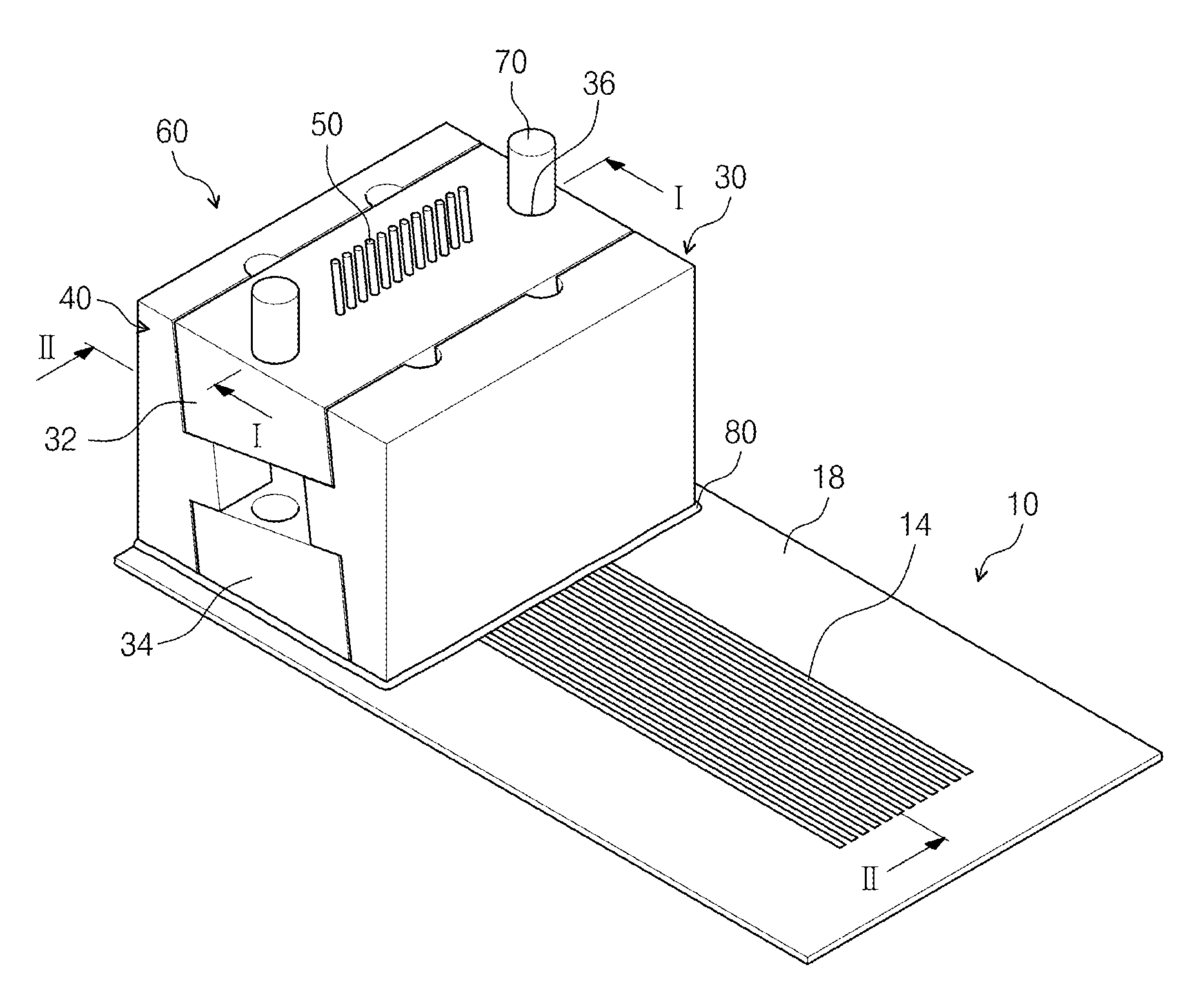
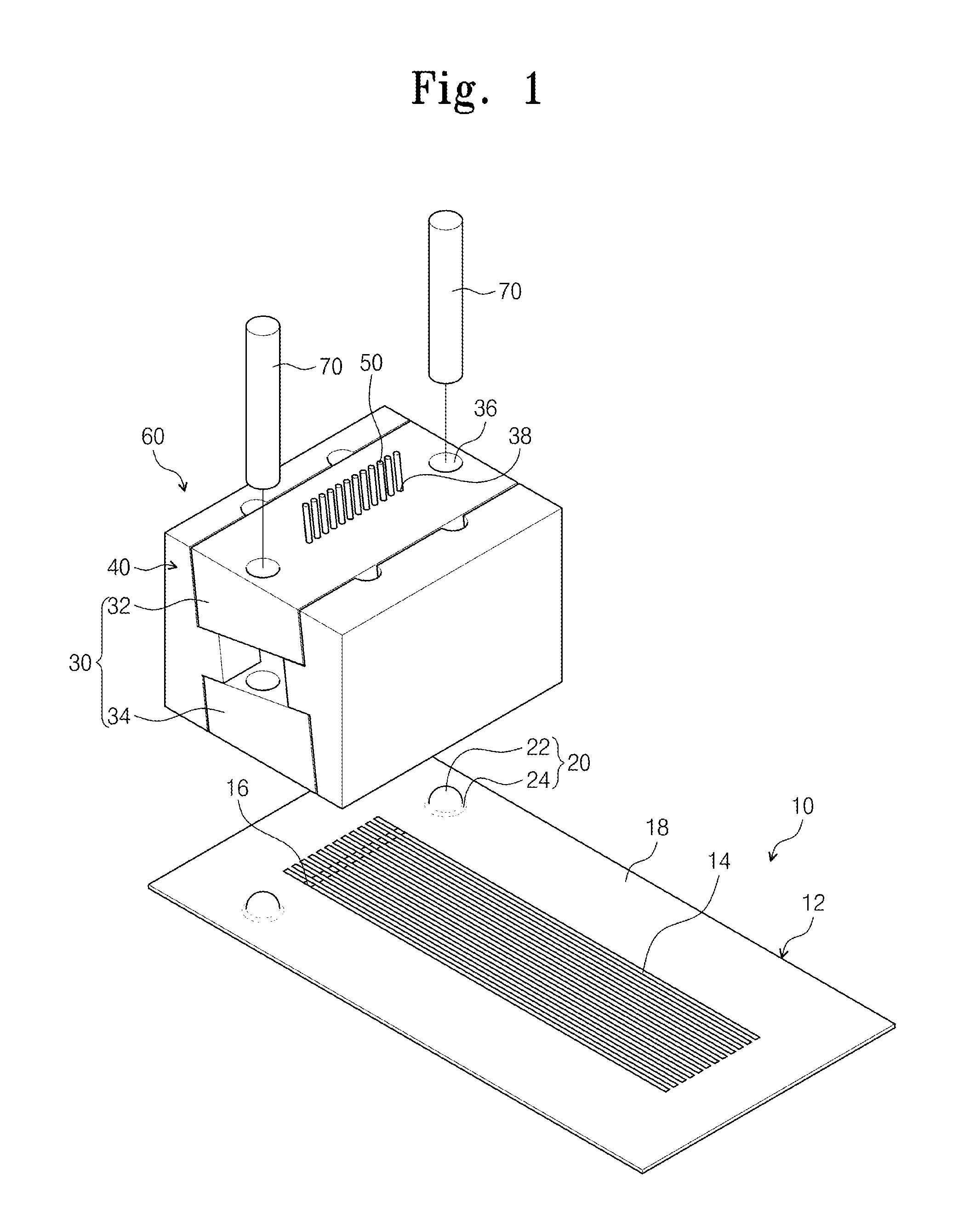
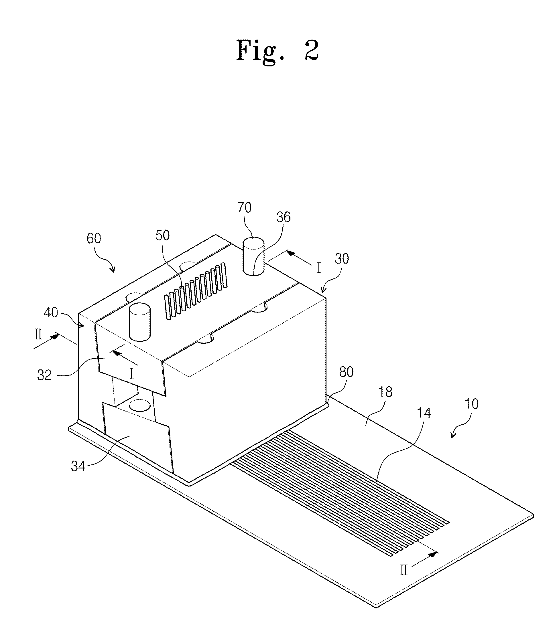
[0031]Preferred embodiments of the present invention will be described below in more detail with reference to the accompanying drawings. Advantages and features of the present invention, and implementation methods thereof will be clarified through following embodiments described with reference to the accompanying drawings. The present invention may, however, be embodied in different forms and should not be construed as limited to the embodiments set forth herein. Rather, these embodiments are provided so that this disclosure will be thorough and complete, and will fully convey the scope of the present invention to those skilled in the art. Further, the present invention is only defined by scopes of claims. Like reference numerals refer to like elements throughout.

[0032]In the following description, the technical terms are used only for explain a specific exemplary embodiment while not limiting the present invention. The terms of a singular form may include plural forms unless referr...


PUM


Abstract

Provided are a photonics chip and an optical apparatus including the same. The chip may include a substrate, an optical waveguide, an optical coupler, and a plurality of alignment units. The optical waveguide is formed on the substrate. The optical coupler is formed at the optical waveguide. The alignment units align an optical connector which fixes at least one optical fiber coupled to the optical coupler, on the substrate.

Description

CROSS-REFERENCE TO RELATED APPLICATIONS[0001]This U.S. non-provisional patent application claims priority under 35 U.S.C. §119 of Korean Patent Application No. 10-2010-0113495, filed on Nov. 15, 2010, the entire contents of which are hereby incorporated by reference.BACKGROUND OF THE INVENTION[0002]The present invention disclosed herein relates to an optical apparatus, and more particularly, to a photonics chip and an optical apparatus having the same.[0003]Optical communication technologies have great potential in terms of being able to transmit high volumes of data at high speed, which is required in IT-oriented society. From thereamong, silicon photonics technology can be used to implement an optical communication system. However, due to the material properties of silicon, silicon photonics are limited, for example, in that silicon photonic light emitting devices cannot be fabricated in monolithic form together other photoelectric devices. An optical connector connected to an ext...

Claims


Application Information

Patent Timeline
Patent Type & Authority Applications(United States)
IPC IPC(8): G02B6/12
CPCG02B6/3644G02B6/4292G02B6/3885G02B6/3652
Inventor KIM, DO WONKIM, GYUNGOCKLEE, JUNYEONG
Owner ELECTRONICS & TELECOMM RES INST
Why Eureka
Try Eureka