Light emitting device and method of fabricating the same

a technology light emitting devices, which is applied in the direction of semiconductor devices, material nanotechnology, electrical devices, etc., can solve the problems of difficult to increase light emission efficiency, difficult to realize the uniformity of quantum dots on the surface of nanorods, and difficult to increase the efficiency of light emitting devices

Active Publication Date: 2012-05-31
SEOUL VIOSYS CO LTD
View PDF3 Cites 30 Cited by
  • Summary
  • Abstract
  • Description
  • Claims
  • Application Information

AI Technical Summary

Benefits of technology

[0012]Various aspects of the present invention provide a light emitting device and a method of fabricating the same, in which the phenomenon of trans

Problems solved by technology

Therefore, it is difficult to increase light emission efficiency.
Moreover, in the light emitting device of the related art, it is difficult to realize the uniformity of quantum dots on the surface of nanor

Method used


Image

  • Light emitting device and method of fabricating the same
  • Light emitting device and method of fabricating the same
  • Light emitting device and method of fabricating the same

Examples


Embodiment Construction

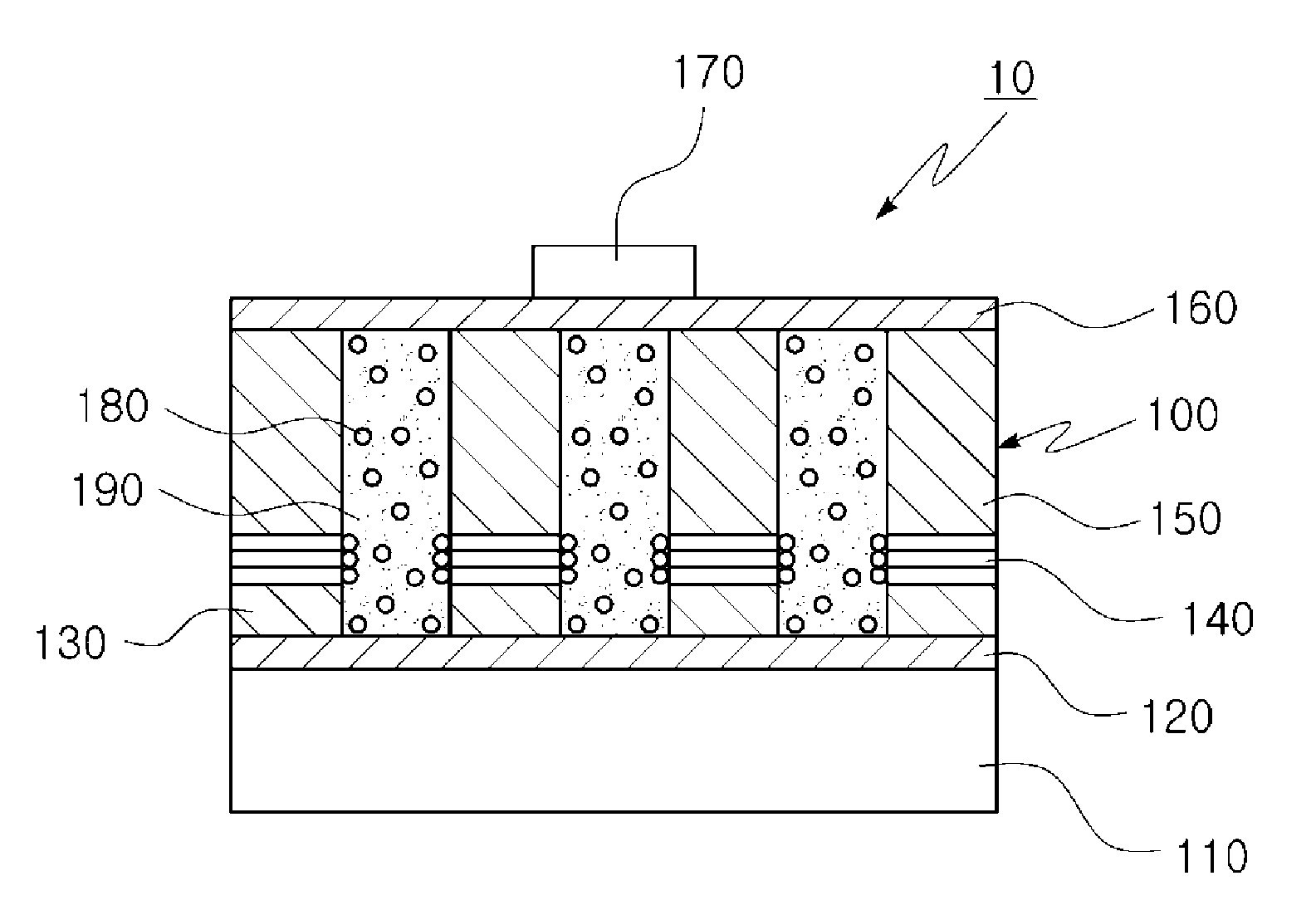
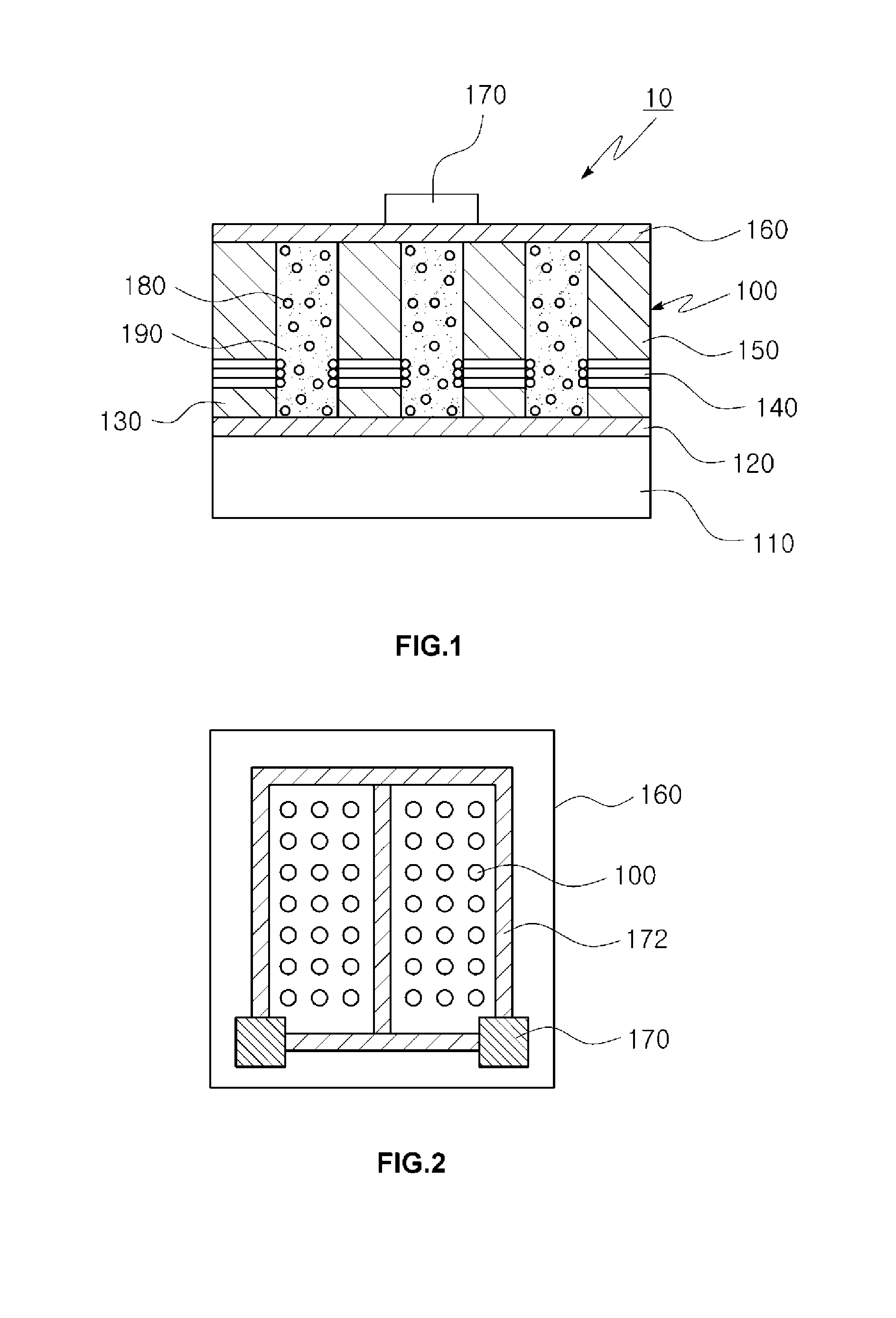
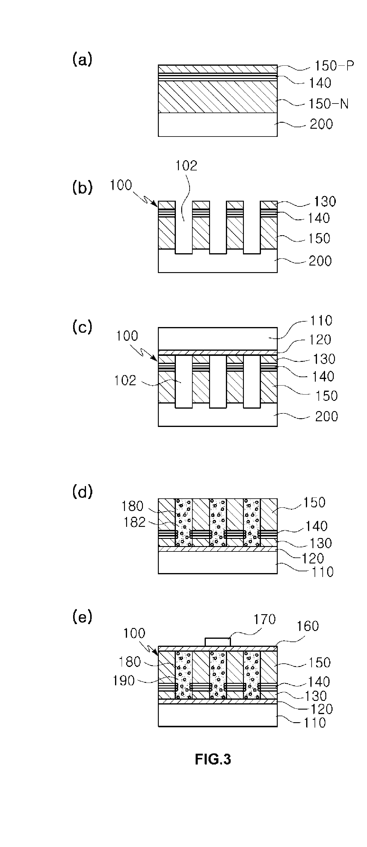
[0028]The present invention will be described more fully hereinafter with reference to the accompanying drawings, in which exemplary embodiments of the invention are shown. This invention may, however, be embodied in many different forms and should not be construed as limited to the embodiments set forth herein. Rather, these embodiments are provided so that this disclosure is thorough, and will fully convey the scope of the invention to those skilled in the art.

[0029]In the drawings, the thickness of layers, films, panels, regions, etc., may be exaggerated for clarity. It will be understood that when an element or layer is referred to as being “on” or “connected to” another element or layer, it can be directly on or directly connected to the other element or layer, or intervening elements or layers may be present. In contrast, when an element is referred to as being “directly on” or “directly connected to” another element or layer, there are no intervening elements or layers presen...


PUM


Abstract

A light emitting device includes a metal backing layer, a reflective electrode layer disposed on the metal backing layer, and a plurality of nanorods disposed on the reflective electrode layer. Each nanorod includes a p-semiconductor layer, an active layer, and an n-semiconductor layer, which are sequentially stacked on the reflective electrode layer. The light emitting device further includes an anti-reflection electrode layer disposed on the nanorods, and quantum dots disposed between the nanorods. The method includes sequentially growing the n-semiconductor layer, the active layer, and the p-semiconductor layer on a substrate; forming the nanorods by etching the p-semiconductor layer using a mask pattern; sequentially forming the reflective electrode layer and the metal backing layer on the p-semiconductor layer and then removing the substrate; disposing quantum dots between the nanorods; and forming the anti-reflection electrode layer on the nanorods.

Description

CROSS REFERENCE TO RELATED APPLICATION[0001]This application claims priority from and the benefit of Korean Patent Application No. 10-2010-0118971 filed on Nov. 26, 2010, which is incorporated herein by reference for all purposes as if fully set forth herein.BACKGROUND OF THE INVENTION[0002]1. Field of the Invention[0003]Exemplary embodiments of the present invention relates to a light emitting device and a method of fabricating the same, and more particularly, to a light emitting device, in which nanorods are disposed such that an active layer is exposed therethrough and quantum dots are distributed between respective nanorods, whereby light emission from the quantum dots may be increased due to energy generated from a Multiple Quantum Well (MQW) structure being is transmitted to the quantum dots, and a method of fabricating the same.[0004]2. Discussion of the Background[0005]A white lighting system typically includes a light emitting device, which emits ultraviolet rays or blue li...

Claims


Application Information

Patent Timeline
IPC IPC(8): H01L33/04H01L29/06B82Y99/00
CPCB82Y30/00H01L33/08H01L33/18B82Y20/00H01L33/502H01L2933/0091H01L33/38
Inventor KWAK, WOO CHULAN, SOON HOKIM, HWA MOKKIM, EUN JINSONG, JAE HOON
Owner SEOUL VIOSYS CO LTD
Why Eureka
Try Eureka